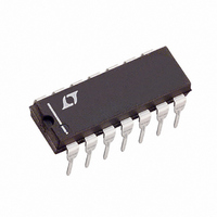
LT1105CN Linear Technology, LT1105CN Datasheet - Page 19

LT1105CN
Manufacturer Part Number
LT1105CN
Description
IC OFFLINE SWIT CM HV 14DIP
Manufacturer
Linear Technology
Datasheet
1.LT1105CN8PBF.pdf
(32 pages)
Specifications of LT1105CN
Output Isolation
Isolated
Frequency Range
20 ~ 200kHz
Voltage - Input
7 ~ 30 V
Voltage - Output
20V
Power (watts)
100W
Operating Temperature
0°C ~ 100°C
Package / Case
14-DIP (0.300", 7.62mm)
Lead Free Status / RoHS Status
Contains lead / RoHS non-compliant
Available stocks
Company
Part Number
Manufacturer
Quantity
Price
Company:
Part Number:
LT1105CN8
Manufacturer:
LT
Quantity:
5 510
Company:
Part Number:
LT1105CN8
Manufacturer:
MAXIM
Quantity:
5 510
Part Number:
LT1105CN8
Manufacturer:
LINEAR/凌特
Quantity:
20 000
Company:
Part Number:
LT1105CN8#PBF
Manufacturer:
AD
Quantity:
11 592
Part Number:
LT1105CN8#PBF
Manufacturer:
LINEAR/凌特
Quantity:
20 000
APPLICATIONS
A special circuit in the LT1103 senses the voltage at V
prior to turning on the switch. V
the FET and should represent the bias voltage on the gate
when the switch is off. When the switch first turns off, the
drain flies back until it is clamped by a snubber network.
The source also flies high due to parasitic capacitive
coupling on the FET and parasitic inductance of the leads.
An extra diode from the source to the gate or V
provide insurance against fault conditions that might
otherwise damage the FET. The diode clamps the source
to one diode drop above the gate or V
the gate source reverse bias. Once the energy in the
leakage inductance spike is dissipated and the primary is
being regulated to its flyback voltage, the diode shuts off.
The source is then floating and its voltage will be close to
the gate voltage. If the sensed voltage on V
10V or greater than 20V, the circuit prevents the switch
from turning on. This protects the FET from dissipating
high power in a nonsaturated state or from excessive gate-
source voltage. The oscillator continues to run and the net
effect is to skip switching cycles until the gate bias voltage
is corrected. One consequence of the gate bias detection
circuit is that the start-up window is 6V if the gate is biased
from V
output. This influences the size of the bypass capacitor on
V
V
The V
NPN power switch. This NPN has a typical on resistance of
0.4 and a typical breakdown voltage (BV
switching times and high efficiency are obtained by using
a special driver loop which automatically adapts base drive
current to the minimum required to keep the switch in a
quasisaturated state. The key element in the loop is an
extra emitter on the output power transistor as seen in the
block diagram. This emitter carries no current when the
NPN output transistor collector is high (unsaturated). In
this condition, the driver circuit can deliver very high base
drive to the switch for fast turn-on. When the switch
saturates, the extra emitter acts as a collector of an NPN
operating in inverted mode and pulls base current away
from the driver. This linear feedback loop serves itself to
IN
SW
.
Output (LT1103)
SW
IN
pin of the LT1103 is the collector of an internal
and to 4V if the gate is biased from the 15V
U
INFORMATION
U
SW
is tied to the source of
W
IN
, thereby limiting
CBO
SW
) of 75V. Fast
is less than
U
IN
will
SW
keep the switch just at the edge of saturation. Very low
switch current results in nearly zero driver current and
high switch currents automatically increase driver current
as necessary. The ratio of switch current to driver current
is approximately 30:1. This ratio is determined by the
sizing of the extra emitter and the value of the current
source feeding the driver circuitry. The quasisaturation
state of the switch permits rapid turn-off without the need
for reverse base emitter voltage drive.
Gate Biasing (LT1105)
The LT1105 is designed to drive an external power MOSFET
in the common source configuration with the totem-pole
output V
flexibility (limited only by the choice of external power
FET) and higher output power applications than allowed by
LT1103. An external, noninductive, power sense resistor
must be used in series with the source of the FET to detect
switch current and must be tied to the input of the current
limit amplifier. The gate needs to be biased at a voltage
high enough to guarantee that the FET is saturated when
the totem-pole gate drive is on. This means 10V as
specified in FET data sheets, plus the totem-pole high side
saturation voltage plus a couple of volts for temperature
variations and processing tolerances. This leads to 15V for
a practical gate bias voltage.
Power MOSFETs are well suited to switching power supplies
because their high speed switching characteristics promote
high switching efficiency. To achieve high switching speed,
the gate capacitance must be charged and discharged
quickly with high peak currents. In particular, the turn-off
current can be as high as the peak switch current. The
switching speed is controlled by the impedance seen by
the gate capacitance. Practically speaking, zero impedance
is not desirable because of the high frequency noise spikes
introduced to the system. The gate bias supply which
drives the totem-pole output stage should be bypassed
with a 1 F low ESR capacitor to ground. This capacitor
supplies the energy to charge the gate capacitance during
gate drive turn-on. The power MOSFET should have a 5
resistor or larger in series with its gate from the V
to define the source impedance.
SW
pin. The advantage is added switch current
LT1103/LT1105
19
SW
pin


