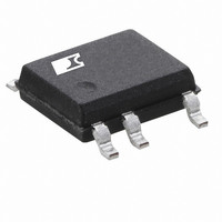
LNK613DG-TL Power Integrations, LNK613DG-TL Datasheet - Page 6

LNK613DG-TL
Manufacturer Part Number
LNK613DG-TL
Description
IC OFFLINE SWIT CV/CC HV 8SOIC
Manufacturer
Power Integrations
Series
LinkSwitch®-IIr
Type
Off Line Switcherr
Datasheet
1.LNK603DG.pdf
(18 pages)
Specifications of LNK613DG-TL
Mfg Application Notes
LinkSwitch-II Family, Appl Note AN-44
Output Isolation
Isolated
Frequency Range
58 ~ 72kHz
Voltage - Output
700V
Power (watts)
3.3W
Operating Temperature
-40°C ~ 150°C
Package / Case
8-SOIC (0.154", 3.90mm Width) 7 leads
Output Voltage
700 V
Input / Supply Voltage (max)
9 V
Input / Supply Voltage (min)
- 0.3 V
Duty Cycle (max)
55 %
Switching Frequency
65 KHz
Supply Current
440 uA
Operating Temperature Range
- 40 C to + 150 C
Mounting Style
SMD/SMT
Maximum Operating Temperature
+ 150 C
Minimum Operating Temperature
- 40 C
Output Current
320 mA
Output Power
3.3 W
For Use With
596-1235 - KIT REF DESIGN LINKSWITCH 2
Lead Free Status / RoHS Status
Lead free / RoHS Compliant
Available stocks
Company
Part Number
Manufacturer
Quantity
Price
Company:
Part Number:
LNK613DG-TL
Manufacturer:
POWER
Quantity:
17 357
Part Number:
LNK613DG-TL
Manufacturer:
POWER
Quantity:
20 000
Figure 5.
Secondary Loop Area
To minimize leakage inductance and EMI the area of the loop
connecting the secondary winding, the output diode and the
output filter capacitor should be minimized. In addition,
sufficient copper area should be provided at the anode and
cathode terminal of the diode for heatsinking. A larger area is
preferred at the quiet cathode terminal. A large anode area can
increase high frequency radiated EMI.
Electrostatic Discharge Spark Gap
An trace is placed along the isolation barrier to form one
electrode of a spark gap. The other electrode on the secondary
is formed by the output return node. The spark gap directs
ESD energy from the secondary back to the AC input. The
trace from the AC input to the spark gap electrode should be
spaced away from other traces to prevent unwanted arcing
occurring and possible circuit damage.
Drain Clamp Optimization
LinkSwitch-II senses the feedback winding on the primary side
to regulate the output. The voltage that appears on the feed-
back winding is a reflection of the secondary winding voltage
while the internal MOSFET is off. Therefore any leakage
inductance induced ringing can affect output regulation. Optimizing
the drain clamp to minimize the high frequency ringing will give
the best regulation. Figure 6 shows the desired drain voltage
waveform compared to Figure 7 with a large undershoot due to
the leakage inductance induced ring. This will reduce the
output voltage regulation performance. To reduce this adjust
the value of the resistor in series with the clamp diode.
Rev. F 01/10
6
LNK603-606/613-616
PCB Layout Example Showing 5.1 W Design Using P Package.
D2
D3
C1
D1
Input Stage
Input
AC
R2
RF1
D4
Feedback
Resistors
L2
R1
Capacitor
Bypass
U1
R1
R6
R3
C2
C4
C5
S
R5
FB
LinkSwitch-II
Primary Clamp
Bypass Supply
S
Components
BP D
C3
S
R4
S
D5
D3
Addition of a Bias Circuit for Higher Light Load Efficiency
and Lower No-load Input Power Consumption.
The addition of a bias circuit can decrease the no-load input
power from ~200 mW down to less than 30 mW at 230 VAC
input. Light load efficiency also increases which may avoid the
need to use a Schottky barrier vs PN junction output diode
while still meeting average efficiency requirements.
The power supply schematic shown in Figure 4 has the bias
circuit incorporated. Diode D6, C5 and R4 form the bias circuit.
As the output voltage is less than 8 V, an additional transformer
winding is needed, AC stacked on top of the feedback winding.
This provides a high enough voltage to supply the BYPASS pin
even during low switching frequency operation at no-load.
In Figure 4 the additional bias winding (from pin 2 to pin 1) is
stacked on top of the feedback winding (pin 4 to pin 2). Diode
D6 rectifies the output and C5 is the filter capacitor. A 10 uF
capacitor is recommended to hold up the bias voltage at low
switching frequencies. The capacitor type is not critical but the
voltage rating should be above the maximum value of V
The recommended current into the BYPASS pin is equal to IC
supply current (~0.5 mA) at the minimum bias winding voltage.
The BYPASS pin current should not exceed 3 mA at the maximum
bias winding voltage. The value of R4 is calculated according to
(V
(0.5 mA typ.) is the IC supply current and V
BIAS
– V
BP
)/I
S2
, where V
T1
Spark
Gap
BIAS
(10 V typ.) is the voltage across C5, I
C8
Diode Snubber
C7
Output
R8
D7
R9
Output
DC
C6
BP
(6.2 V typ.) is the
Output Filter
www.powerint.com
Capacitors
Resistor
Preload
PI-5110-050508
BIAS
.
S2


