LNK625DG-TL Power Integrations, LNK625DG-TL Datasheet - Page 10
LNK625DG-TL
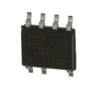
Manufacturer Part Number
LNK625DG-TL
Description
IC OFFLINE SWIT OTP OCP CV 8SOP
Manufacturer
Power Integrations
Series
LinkSwitch®-CVr
Datasheet
1.LNK625DG.pdf
(18 pages)
Specifications of LNK625DG-TL
Output Isolation
Isolated
Frequency Range
93 ~ 106kHz
Voltage - Output
700V
Power (watts)
13.5W
Operating Temperature
-40°C ~ 150°C
Package / Case
8-SOIC (0.154", 3.90mm Width) 7 leads
Duty Cycle (max)
54 %
Operating Temperature Range
- 40 C to + 150 C
Mounting Style
SMD/SMT
Maximum Operating Temperature
+ 150 C
Minimum Operating Temperature
- 40 C
Number Of Outputs
3
Output Power
8 W
Lead Free Status / RoHS Status
Lead free / RoHS Compliant
Available stocks
Company
Part Number
Manufacturer
Quantity
Price
Company:

Part Number:
LNK625DG-TL
Manufacturer:
POWER
Quantity:
15 000
Company:
Part Number:
LNK625DG-TL
Manufacturer:
PowerInt
Quantity:
7 160
Part Number:
LNK625DG-TL
Manufacturer:
POWER
Quantity:
20 000


Rev. E 09/09
The following minimum set of tests is strongly recommended:
1. Maximum drain voltage – Verify that peak V
2. Maximum drain current – At maximum ambient temperature,
10
680 V at highest input voltage and maximum output power.
maximum input voltage and maximum output load, verify
drain current waveforms at start-up for any signs of trans-
former saturation and excessive leading edge current spikes.
LinkSwitch-CV has a leading edge blanking time of 215 ns to
prevent premature termination of the ON-cycle. Verify that
the leading edge current spike is below the allowed current
limit envelope for the drain current waveform at the end of
the 215 ns blanking period.
LNK623-626
DS
does not exceed
3. Thermal check – At maximum output power, both minimum
Design Tools
Up-to-date information on design tools can be found at the
Power Integrations web site: www.powerint.com
and maximum input voltage and maximum ambient tempera-
ture; verify that temperature specifi cations are not exceeded
for LinkSwitch-CV, transformer, output diodes and output
capacitors. Enough thermal margin should be allowed for
the part-to-part variation of the R
specifi ed in the data sheet. It is recommended that the
maximum source pin temperature does not exceed 110 °C.
DS(ON)
of LinkSwitch-CV, as
www.powerint.com
Related parts for LNK625DG-TL
Image
Part Number
Description
Manufacturer
Datasheet
Request
R

Part Number:
Description:
SOP-16
Manufacturer:
Power Integrations
Datasheet:
Part Number:
Description:
DIP8
Manufacturer:
Power Integrations
Datasheet:
Part Number:
Description:
TO-263
Manufacturer:
Power Integrations
Datasheet:
Part Number:
Description:
TO-263
Manufacturer:
Power Integrations
Datasheet:
Part Number:
Description:
Manufacturer:
Power Integrations
Datasheet: