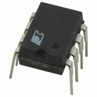
TNY253PN Power Integrations, TNY253PN Datasheet - Page 2

TNY253PN
Manufacturer Part Number
TNY253PN
Description
IC OFFLINE SWIT OTP OCP HV 8DIP
Manufacturer
Power Integrations
Series
TinySwitch®r
Datasheet
1.TNY253GN-TL.pdf
(20 pages)
Specifications of TNY253PN
Output Isolation
Isolated
Frequency Range
40 ~ 48kHz
Voltage - Output
700V
Power (watts)
2W
Operating Temperature
-40°C ~ 150°C
Package / Case
8-DIP (0.300", 7.62mm)
Output Voltage
5.8 V
Input / Supply Voltage (max)
265 VAC
Input / Supply Voltage (min)
85 VAC
Duty Cycle (max)
68 %
Switching Frequency
44 KHz
Supply Current
140 uA
Operating Temperature Range
- 40 C to + 150 C
Mounting Style
Through Hole
Lead Free Status / RoHS Status
Lead free / RoHS Compliant
Available stocks
Company
Part Number
Manufacturer
Quantity
Price
Company:
Part Number:
TNY253PN
Manufacturer:
FREESCALE
Quantity:
652
Part Number:
TNY253PN
Manufacturer:
POWER
Quantity:
20 000
Figure 2. Functional Block Diagram.
Pin Functional Description
DRAIN (D) Pin:
Power MOSFET drain connection. Provides internal operating
current for both start-up and steady-state operation.
BYPASS (BP) Pin:
Connection point for an external bypass capacitor for the
internally generated 5.8 V supply. Bypass pin is not intended
for sourcing supply current to external circuitry.
ENABLE (EN) Pin:
The power MOSFET switching can be terminated by pulling
this pin low. The I-V characteristic of this pin is equivalent to
a voltage source of approximately 1.5 V with a source current
clamp of 50 µA.
SOURCE (S) Pin:
Power MOSFET source connection. Primary return.
TinySwitch Functional Description
TinySwitch is intended for low power off-line applications. It
combines a high voltage power MOSFET switch with a power
supply controller in one device. Unlike a conventional PWM
(Pulse Width Modulator) controller, the TinySwitch uses a
simple ON/OFF control to regulate the output voltage.
The TinySwitch controller consists of an Oscillator, Enable
(Sense and Logic) circuit, 5.8 V Regulator, Under-Voltage
BYPASS
TNY253/254/255
ENABLE
2
D
4/03
50 A
1.5 V + V TH
OSCILLATOR
DC MAX
CLOCK
5.8 V
5.1 V
SHUTDOWN
THERMAL
+
-
S
R
UNDER-VOLTAGE
circuit, Hysteretic Over Temperature Protection, Current Limit
circuit, Leading Edge Blanking, and a 700 V power MOSFET.
Figure 2 shows a functional block diagram with the most
important features.
Oscillator
The oscillator frequency is internally set at 44 kHz (130 kHz for
the TNY255). The two signals of interest are the Maximum
Duty Cycle signal (D
cycle and the Clock signal that indicates the beginning of each
cycle. When cycles are skipped (see below), the oscillator
frequency doubles (except for TNY255 which remains at
130 kHz). This increases the sampling rate at the ENABLE pin
for faster loop response.
Enable (Sense and Logic)
The ENABLE pin circuit has a source follower input stage set
at 1.5 V. The input current is clamped by a current source set
at 50 µA with 10 µA hysteresis. The output of the enable sense
Figure 3. Pin Configuration.
Q
Q
SOURCE
SOURCE
BYPASS
ENABLE
REGULATOR
5.8 V
G Package (SMD-8)
MAX
P Package (DIP-8)
2
1
3
4
) which runs at typically 67% duty
BLANKING
LEADING
EDGE
+
-
8
6
5
7
SOURCE
SOURCE
SOURCE
DRAIN
V I
LIMIT
PI-2199-031501
PI-2197-061898
DRAIN
SOURCE


