PKS605YN Power Integrations, PKS605YN Datasheet - Page 10
PKS605YN
Manufacturer Part Number
PKS605YN
Description
IC OFFLINE SWIT OTP OCP HV TO220
Manufacturer
Power Integrations
Series
PeakSwitch®r
Specifications of PKS605YN
Mfg Application Notes
PeakSwitch Design Guide AppNote
Output Isolation
Isolated
Frequency Range
250 ~ 304kHz
Voltage - Output
700V
Power (watts)
79W
Operating Temperature
-40°C ~ 150°C
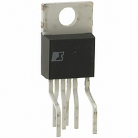
Package / Case
TO-220-7 (Formed Leads), 5 Leads
Output Voltage
24 V
Input / Supply Voltage (max)
265 VAC
Input / Supply Voltage (min)
85 VAC
Duty Cycle (max)
65 %
Switching Frequency
47 KHz
Supply Current
25 uA
Operating Temperature Range
- 40 C to + 150 C
Mounting Style
Through Hole
For Use With
596-1126 - KIT DESIGN ACC PEAKSWITCH FAMILY
Lead Free Status / RoHS Status
Lead free / RoHS Compliant
Other names
596-1121-5
Available stocks
Company
Part Number
Manufacturer
Quantity
Price
Company:

Part Number:
PKS605YN
Manufacturer:
POWER
Quantity:
15 000


Power (W)
Figure 16. Continuous (Average) Output Power Calculation
Figure 16 shows how to calculate the average power
requirements for a design with two different peak load conditions.
Where P
durations of each peak power condition, and T is the period of
one cycle of the pulse load condtion.
Audible Noise
The cycle skipping mode of operation used in PeakSwitch
can generate audio frequency components in the transformer.
To limit this audible noise generation, the transformer should
be designed such that the peak core flux density is below
3000 Gauss (300 mT). Following this guideline and using the
standard transformer production technique of dip varnishing
practically eliminates audible noise. Vacuum impregnation
of the transformer should not be used due to the high primary
capacitance and increased losses that result.
Ceramic capacitors that use dielectrics such as Z5U, when used
in clamp circuits, may also generate audio noise. If this is the
case try replacing them with a capacitor having a different type of
dielectric or construction, for example a film type capacitor.
Maximum Flux Density
A maximum value of 3000 Gauss during normal operation is
recommended to limit the maximum flux density under start
up and output short circuit. Under these conditions the output
voltage is low and little reset of the transformer occurs during
the MOSFET off time. This allows the transformer flux density
to staircase above the normal operating level. A value of
3000 Gauss at the peak current limit of the selected device,
together with the built in protection features of PeakSwitch
Rev. I 02/07
10
P
P
P
3
2
1
X
are the different output power conditions, Δt
Example.
PKS603-607
∆t
1
T
∆t
2
X
are the
Time (t)
provides sufficient margin to prevent core saturation under
startup or output short circuit conditions.
Optocoupler CTR
To minimize the delay introduced by the optocoupler, it is
recommended that a high (300-600%) CTR optocoupler is used
in PeakSwitch designs.
Bias Winding
All PeakSwitch designs must use a bias winding to feed operating
current into the BYPASS pin once the supply is operational.
It is recommended that the value of the resistor from the bias
winding to the BYPASS pin be selected such that it supplies the
same current as the maximum datasheet drain supply current
(I
PeakSwitch Layout Considerations
See Figure 17 for a recommended circuit board layout for
PeakSwitch.
Single Point Grounding
Devices in Y and F packages have separate return pins for the
MOSFET source (S) and the controller (GND) connections
which are internally connected. Therefore connecting these
pins on the PC board is not recommended.
Devices in the P package do not have separate return pins,
but in both cases the low current feedback signals and IC
decoupling, high MOSFET current and bias winding primary
return connection should route through separate traces to the
Kelvin connection.
The bias winding return connection is treated separately, even
though it carries low current. To route high currents away from
the device when the supply is subjected to line surge transients,
the bias winding should be returned directly to the input bulk
capacitor.
Bypass Capacitor (C
The BYPASS pin capacitor should be located as close as possible
to the BYPASS and SOURCE pins.
Primary Loop Area
The area of the primary loop that connects the input filter
capacitor, transformer primary and PeakSwitch together should
be kept as small as possible.
Primary Clamp Circuit
A clamp is used to limit the peak voltage on the DRAIN pin
at turn off. This can be achieved by using an RCD clamp or a
Zener (~200 V) and diode clamp across the primary winding.
In all cases to minimize EMI care should be taken to minimize
the circuit path from the clamp components to the transformer
and PeakSwitch.
S2
) for the specific device being used.
BP
)
Related parts for PKS605YN
Image
Part Number
Description
Manufacturer
Datasheet
Request
R

Part Number:
Description:
SOP-16
Manufacturer:
Power Integrations
Datasheet:
Part Number:
Description:
DIP8
Manufacturer:
Power Integrations
Datasheet:
Part Number:
Description:
TO-263
Manufacturer:
Power Integrations
Datasheet:
Part Number:
Description:
TO-263
Manufacturer:
Power Integrations
Datasheet:
Part Number:
Description:
Manufacturer:
Power Integrations
Datasheet: