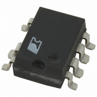
LNK500G-TL Power Integrations, LNK500G-TL Datasheet - Page 4

LNK500G-TL
Manufacturer Part Number
LNK500G-TL
Description
IC SWIT OCP CV/CC HV 8SMD
Manufacturer
Power Integrations
Series
LinkSwitch®r
Datasheet
1.LNK500PN.pdf
(20 pages)
Specifications of LNK500G-TL
Output Isolation
Isolated
Frequency Range
24 ~ 49.5kHz
Voltage - Output
700V
Power (watts)
5.5W
Operating Temperature
-40°C ~ 150°C
Package / Case
8-SMD Gull Wing, 7 Leads
Lead Free Status / RoHS Status
Contains lead / RoHS non-compliant
The characteristics described above provide an approximate
CV/CC power supply output without the need for secondary-
side voltage or current feedback. The output voltage regulation
is influenced by how well the voltage across C2 tracks the
reflected output voltage. This tracking is influenced by the
value of the transformer leakage inductance which introduces
an error. Resistor R2 and capacitor C2 partially filter the
leakage inductance voltage spike reducing this error. This
circuitry, used with standard transformer construction
techniques provides much better output load regulation than a
linear transformer, making this an ideal power supply solution
in many low power applications. If tighter load regulation is
required, an optocoupler configuration can be used while still
employing the constant output current characteristics provided
by LinkSwitch.
Optional Secondary Feedback
Figure 6 shows a typical power supply outline schematic using
LinkSwitch with optocoupler feedback to improve output
voltage regulation. On the primary side, the schematic differs
Figure 7. Influence of the Optocoupler on the Power Supply Output Characteristic.
Figure 6. Power Supply Outline Schematic with Optocoupler Feedback.
threshold
feedback
4
Voltage
85-265
VAC
LNK500
Output Voltage
D
2/05
Load variation
during battery
charging
LNK500
LinkSwitch
D
R1
R2
D1
R3
C
transition
CC to CV
Inherent
point
Output Current
S
from Figure 5 by the addition of R3, C3 and optocoupler U1.
R3 forms a potential divider with R1 to limit the U1 collector
emitter voltage.
On the secondary side, the addition of voltage sense circuit
components R4, VR1 and U1 LED provide the voltage feedback
signal. In the example shown, a simple Zener (VR1) reference
is used though a precision TL431 reference is typically needed
to provide ±5% output voltage tolerancing and cable drop
compensation, if required. Resistor R4 provides biasing for VR1.
The regulated output voltage is equal to the sum of the VR1
Zener voltage plus the forward voltage drop of the U1 LED.
Resistor R5 is an optional low value resistor to limit U1 LED
peak current due to output ripple. Manufacturerʼs specifications
for U1 current and VR1 slope resistance should be consulted
to determine whether R5 is required.
U1 is arranged with collector connected to primary ground and
emitter to the anode of D1. This connection keeps the opto in
an electrically “quiet” position in the circuit. If the opto was
C3
C1
U1
C2
characteristic without
without optocoupler
Tolerance envelope
Characteristic with
Typical inherent
optocoupler
optocoupler
U1
R5
VR1
R4
PI-2788-092101
PI-3418-071304
V
RTN
OUT


