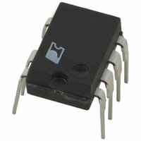
LNK501P Power Integrations, LNK501P Datasheet

LNK501P
Specifications of LNK501P
Available stocks
Related parts for LNK501P
LNK501P Summary of contents
Page 1
... Optional Secondary Feedback section. Figure 1. Typical Application – Not a Simplified Circuit (a) and PRODUCT LNK501P or G Table 1. Notes: 1. Typical output power for designs in an enclosed adapter measured at 50 °C ambient. 2. Uses higher reflected voltage transformer designs for increased power capability – See Key Application Considerations section ...
Page 2
LNK501 CONTROL SHUNT REGULATOR/ ERROR AMPLIFIER - 5 OSCILLATOR D MAX CLOCK SAW I DCS R E Figure 2. Block Diagram. Pin Functional Description DRAIN (D) Pin: Power MOSFET drain connection. Provides ...
Page 3
LinkSwitch Functional Description The duty cycle, current limit and operating frequency relationships with CONTROL pin current are shown in Figure 4. Figure 5 shows a typical power supply outline schematic which is used below to describe the LinkSwitch operation. Power ...
Page 4
LNK501 The characteristics described above provide an approximate CV/CC power supply output without the need for secondary side voltage or current feedback. The output voltage regulation is influenced by how well the voltage across C2 tracks the reflected output voltage. ...
Page 5
D1, it would become a switching node, generating additional common mode EMI currents through its internal parasitic capacitance. The feedback configuration in Figure 6 is simply a resistive divider made ...
Page 6
LNK501 However, in laboratory bench tests often more convenient to test the power supply output characteristic starting from a low output current and gradually increasing the load. In this case, the optocoupler feedback regulates the output voltage until ...
Page 7
BR1 1 A, 600 V RF1 10 Ω Fusible C1 4.7 µF 85-265 400 V VAC Figure 9. 2.75 W Constant Voltage/Constant Current (CV/CC) Charger using LinkSwitch ...
Page 8
LNK501 3. A secondary output with a Schottky rectifier diode. 4. Assumed efficiency of 70%. 5. The part is board mounted with SOURCE pins soldered to sufficient area of copper to keep the die temperature at or ...
Page 9
At very light or no-load, typically less than output current, the output voltage rises due to leakage inductance peak charging of the secondary. This voltage rise can be reduced with a small preload with little change to ...
Page 10
... If this does not occur then the design should be refined to ensure the overall tolerance limits are met. Design Tools Up to date information on design tools can be found at the Power Integrations website: www.powerint.com LinkSwitch ...
Page 11
DRAIN Voltage .................................. ................ -0 700 V DRAIN Peak Current......................................400 mA CONTROL Voltage ................................................ -0 CONTROL Current (not to exceed 9 V)............100 mA Storage Temperature .......................................... -65 °C to 150 °C ..................... -40 °C ...
Page 12
LNK501 Parameter Symbol SHUTDOWN/AUTO-RESTART CONTROL Pin I Charging Current C(CH) I Control/Supply/ CD1 Discharge Current I CD2 Auto-Restart V Threshold Voltage C(AR) Auto-Restart V Hysteresis Voltage C(AR)hyst Auto-Restart Duty DC Cycle (AR) Auto-Restart f Frequency (AR) CIRCUIT PROTECTION Self-Protection I ...
Page 13
Parameter Symbol OUTPUT ON-State R Resistance DS(ON) OFF-State Drain I Leakage Current DSS Breakdown Voltage BV DSS DRAIN Supply Voltage NOTES: A. For specifications with negative values, a negative temperature coefficient corresponds to an increase in magnitude with increasing temperature, ...
Page 14
LNK501 Figure 12. LinkSwitch General Test Circuit 5. 1.6 1.2 0.8 0 DRAIN Voltage (V) Figure 13. I vs. DRAIN Voltage. C 120 100 ...
Page 15
Typical Performance Characteristics 1.1 1.0 0.9 -50 - 100 125 150 Junction Temperature (°C) Figure 17. Breakdown Voltage vs. Temperature. 1.200 1.000 0.800 0.600 0.400 0.200 0.000 -50 - 100 125 150 ...
Page 16
LNK501 Typical Performance Characteristics (cont 2/05 300 =25 °C T CASE =100 °C T 250 CASE 200 150 100 Drain Voltage (V) Figure 23. Output Characteristics (DRAIN Current vs. DRAIN Voltage). ...
Page 17
PART ORDERING INFORMATION LNK 501 ⊕ .004 (.10) -E- .240 (6.10) .260 (6.60) Pin 1 .367 (9.32) -D- .387 (9.83) .125 (3.18) .145 (3.68) -T- SEATING PLANE .100 (2.54) BSC .048 (1.22) .053 (1.35) ...
Page 18
LNK501 ⊕ .004 (.10) -E- .240 (6.10) .260 (6.60) Pin 1 .100 (2.54) (BSC) .367 (9.32) -D- .387 (9.83) .125 (3.18) .145 (3.68) .032 (.81) .048 (1.22) .037 (.94) .053 (1.35 2/05 SMD-8B .137 (3.48) MINIMUM ...
Page 19
Revision Notes D 1) Released Final Data Sheet Enhanced tolerance with optocoupler designs. 2) Updated P and G packages thermal impedance Corrected minor errors in text and figures. 2) Updated Figure 6 and text description. G ...
Page 20
... For the latest updates, visit our website: www.powerint.com Power Integrations reserves the right to make changes to its products at any time to improve reliability or manufacturability. Power Integrations does not assume any liability arising from the use of any device or circuit described herein. POWER INTEGRATIONS MAKES NO WARRANTY HEREIN AND SPECIFICALLY DISCLAIMS ALL WARRANTIES INCLUDING, WITHOUT LIMITATION, THE IMPLIED WARRANTIES OF MERCHANTABILITY, FITNESS FOR A PARTICULAR PURPOSE, AND NON-INFRINGEMENT OF THIRD PARTY RIGHTS ...


