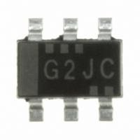
S-8261AAJMD-G2JT2G Seiko Instruments, S-8261AAJMD-G2JT2G Datasheet - Page 21

S-8261AAJMD-G2JT2G
Manufacturer Part Number
S-8261AAJMD-G2JT2G
Description
IC BATT PROTECTION 1CELL SOT23-6
Manufacturer
Seiko Instruments
Datasheet
1.S-8261AAJMD-G2JT2G.pdf
(33 pages)
Specifications of S-8261AAJMD-G2JT2G
Function
Over/Under Voltage Protection
Battery Type
Lithium-Ion (Li-Ion), Lithium-Polymer (Li-Pol)
Operating Temperature
-40°C ~ 85°C
Mounting Type
Surface Mount
Package / Case
SOT-23-6
Product
Li-Ion Protection
Output Voltage
8 V
Operating Supply Voltage
1.5 V to 8 V
Supply Current
7 uA
Maximum Operating Temperature
+ 85 C
Minimum Operating Temperature
- 40 C
Mounting Style
SMD/SMT
Uvlo Start Threshold
1 V
Lead Free Status / RoHS Status
Lead free / RoHS Compliant
Other names
728-1034-2
Available stocks
Company
Part Number
Manufacturer
Quantity
Price
Company:
Part Number:
S-8261AAJMD-G2JT2G
Manufacturer:
SEIKO
Quantity:
93 000
Part Number:
S-8261AAJMD-G2JT2G
Manufacturer:
SEIKO/精工
Quantity:
20 000
Rev.5.0
8. DP Pin
9. 0 V Battery Charging Function “Available”
10. 0 V Battery Charging Function “Unavailable”
The DP pin is a test pin for delay time measurement and it should be open in the actual application. If a capacitor
whose capacitance is larger than 1000 pF or a resistor whose resistance is less than 1 MΩ is connected to this pin,
error may occur in the delay times or in the detection voltages.
This function is used to recharge the connected battery whose voltage is 0 V due to the self-discharge. When the 0 V
battery charge starting charger voltage (V
charger, the charging control FET gate is fixed to VDD pin voltage. When the voltage between the gate and source
of the charging control FET becomes equal to or higher than the turn-on voltage due to the charger voltage, the
charging control FET is turned on to start charging. At this time, the discharging control FET is off and the charging
current flows through the internal parasitic diode in the discharging control FET. When the battery voltage becomes
equal to or higher than the overdischarge detection voltage (V
S-8261 Series enters the normal status.
Caution
Remark
This function inhibits the recharging when a battery that is short-circuited (0 V battery) internally is connected. When
the battery voltage is the 0 V battery charge inhibition battery voltage (V
is fixed to EB− pin voltage to inhibit charging. When the battery voltage is the 0 V battery charge inhibition battery
voltage (V
Caution
_00
0INH
Some battery providers do not recommend charging for completely self-discharged battery.
Please ask battery providers before determine whether to enable or inhibit the 0 V battery charging
function.
The 0 V battery charge function has higher priority than the abnormal charge current detection function.
Consequently, a product with the 0 V battery charging function is enabled charges a battery forcibly and
abnormal charge current cannot be detected when the battery voltage is low.
Some battery providers do not recommend charging for completely self-discharged battery.
Please ask battery providers before determining the 0 V battery charging function.
) or higher, charging can be performed.
0CHA
Seiko Instruments Inc.
) or higher is applied between EB+ pin and EB− pin by connecting a
LOW DROPOUT CMOS VOLTAGE REGULATOR
DL
) and the overdischarge hysteresis voltage (V
0INH
) or lower, the charging control FET gate
S-8261 Series
HD
), the
21


