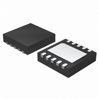
LTC4080EDD#TRPBF Linear Technology, LTC4080EDD#TRPBF Datasheet - Page 13

LTC4080EDD#TRPBF
Manufacturer Part Number
LTC4080EDD#TRPBF
Description
IC CHARGER LI-ION 10-DFN
Manufacturer
Linear Technology
Datasheet
1.LTC4080EMSEPBF.pdf
(20 pages)
Specifications of LTC4080EDD#TRPBF
Function
Charge Management
Battery Type
Lithium-Ion (Li-Ion)
Voltage - Supply
3.75 V ~ 5.5 V
Operating Temperature
-40°C ~ 85°C
Mounting Type
Surface Mount
Package / Case
10-WFDFN Exposed Pad
Lead Free Status / RoHS Status
Lead free / RoHS Compliant
Available stocks
Company
Part Number
Manufacturer
Quantity
Price
OPERATIO
from zero to full-scale current over a period of approximately
180μs. This has the effect of minimizing the transient cur-
rent load on the power supply during start-up.
Timer and Recharge
The LTC4080’s battery charger has an internal termina-
tion timer that starts when the input voltage is greater
than the undervoltage lockout threshold and at least
80mV above BAT, and the battery charger is leaving
shutdown.
At power-up or when exiting shutdown, the charge time
is set to 4.5 hours. Once the charge cycle terminates, the
battery charger continuously monitors the BAT pin voltage
using a comparator with a 2ms fi lter time. When the aver-
age battery voltage falls below 4.1V (which corresponds
to 80%-90% battery capacity), a new charge cycle is initi-
ated and a 2.25 hour timer begins. This ensures that the
battery is kept at, or near, a fully charged condition and
eliminates the need for periodic charge cycle initiations.
The ⎯ C ⎯ H ⎯ R ⎯ G output assumes a strong pulldown state dur-
ing recharge cycles until C/10 is reached or the recharge
cycle terminates.
SWITCHING REGULATOR OPERATION:
The switching regulator in the LTC4080 can be turned on
by pulling the EN_BUCK pin above V
selectable modes of operation: constant-frequency (PWM)
mode and Burst Mode Operation. The constant-frequency
mode operation offers low noise at the expense of effi -
ciency whereas the Burst Mode operation offers increased
effi ciency at light loads at the cost of increased noise and
output voltage ripple. A detailed description of different
operating modes and different aspects of operation fol-
low. Operations can best be understood by referring to
the Block Diagram.
Constant-Frequency (PWM) Mode Operation
The switching regulator operates in constant-frequency
(PWM) mode when the MODE pin is pulled below V
this mode, it uses a current mode architecture including
an oscillator, an error amplifi er, and a PWM comparator
for excellent line and load regulation. The main switch
MP2 (P-channel MOSFET) turns on to charge the inductor
U
IH
. It has two user-
IL
. In
at the beginning of each clock cycle if the FB pin voltage
is less than the 0.8V reference voltage. The current into
the inductor (and the load) increases until it reaches the
peak current demanded by the error amp. At this point,
the main switch turns off and the synchronous switch
MN1 (N-channel MOSFET) turns on allowing the inductor
current to fl ow from ground to the load until either the
next clock cycle begins or the current reduces to the zero
current (I
Oscillator: In constant-frequency mode, the switching
regulator uses a dedicated oscillator which runs at a
fi xed frequency of 2.25MHz. This frequency is chosen to
minimize possible interference with the AM band.
Error Amplifi er: The error amplifi er is an internally com-
pensated transconductance (g
of 65 μmhos. The internal 0.8V reference voltage is
compared to the voltage at the FB pin to generate a
current signal at the output of the error amplifi er. This
current signal is then converted into a voltage signal
(I
to achieve regulation.
PWM Comparator: Lossless current sensing converts the
PMOS switch current signal to a voltage which is summed
with the internal slope compensation signal. The PWM
comparator compares this summed signal to I
determines when to turn off the main switch. The switch
current sensing is blanked for ~12ns at the beginning of
each clock cycle to prevent false switch turn-off.
Burst Mode Operation
Burst Mode operation can be selected by pulling the
MODE pin above V
lator is disabled, the error amplifi er is converted into a
comparator monitoring the FB voltage, and the inductor
current swings between a fi xed I
(35mA) irrespective of the load current as long as the FB
pin voltage is less than or equal to the reference voltage
of 0.8V. Once V
shuts off both switches along with most of the circuitry
and the regulator is said to enter into SLEEP mode. In
SLEEP mode, the regulator only draws about 20μA from
the BAT pin provided that the battery charger is turned
off. When the output voltage droops about 1% from its
TH
), and represents the peak inductor current required
ZERO
) level.
FB
is greater than 0.8V, the control logic
IH
. In this mode, the internal oscil-
m
PEAK
) amplifi er with a g
(~80mA) and I
LTC4080
13
TH
ZERO
4080fb
and
m


