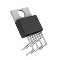
LT1513-2IT7#PBF Linear Technology, LT1513-2IT7#PBF Datasheet - Page 5

LT1513-2IT7#PBF
Manufacturer Part Number
LT1513-2IT7#PBF
Description
IC BATT CHG CNST/PROG I/V TO2207
Manufacturer
Linear Technology
Datasheet
1.LT1513-2CR.pdf
(16 pages)
Specifications of LT1513-2IT7#PBF
Function
Charge Management
Battery Type
All Battery Types
Voltage - Supply
2.7 V ~ 25 V
Operating Temperature
-40°C ~ 125°C
Mounting Type
Through Hole
Package / Case
TO-220-7 Formed Leads
Lead Free Status / RoHS Status
Lead free / RoHS Compliant
Available stocks
Company
Part Number
Manufacturer
Quantity
Price
PIN
V
frequency compensation, but it can also be used for soft
starting and current limiting. It is the output of the error
amplifier and the input of the current comparator. Peak
switch current increases from 0A to 3.6A as the V
varies from 1V to 1.9V. Current out of the V
200 A when the pin is externally clamped below the
internal 1.9V clamp level. Loop frequency compensation
is performed with a capacitor or series RC network from
the V
FB (Pin 2): The feedback pin is used for positive output
voltage sensing. The R1/R2 voltage divider connected to
FB defines Li-Ion float voltage at full charge, or acts as a
voltage limiter for NiCd or NiMH applications. FB is the
inverting input to the voltage error amplifier. Input bias
current is typically 300nA, so divider current is normally
set to 100 A to swamp out any output voltage errors due
to bias current. The noninverting input of this amplifier is
tied internally to a 1.245V reference. The grounded end of
the output voltage divider should be connected directly to
the LT1513 ground pin (avoid ground loops).
I
charging current. It is the input to a current sense amplifier
that controls charging current when the battery voltage is
below a programmed limit. During constant-current
operation, the LT1513 I
resistance of this pin is 5k , so filter resistance (R4,
Figure 1) should be less than 50 . The 39 , 0.22 F filter
shown in Figure 1 is used to convert the pulsating current
in the sense resistor to a smooth DC current feedback
signal. The LT1513-2 I
programmable current limit. The current through R5,
Figure 5, is balanced by the current through R4, program-
ming the maximum voltage across R3.
FB
C
U
(Pin 1): The compensation pin is primarily used for
(Pin 3): The current feedback pin is used to sense
C
pin directly to the ground pin (avoid ground loops).
FUNCTIONS
U
U
FB
FB
pin regulates at 0mV to provide
pin regulates at – 100mV. Input
C
pin is about
C
voltage
GND (Pin 4): The ground pin is common to both control
circuitry and switch current. V
be Kelvin and connected as close as possible to this pin.
The TAB of the R package should also be connected to the
power ground.
V
switch, carrying up to 3A of current with fast rise and fall
times. Keep the traces on this pin as short as possible to
minimize radiation and voltage spikes. In particular, the
path in Figure 1 which includes SW to C2, D1, C1 and
around to the LT1513 ground pin should be as short as
possible to minimize voltage spikes at switch turn-off.
S/S (Pin 6): This pin can be used for shutdown and/or
synchronization. It is logic level compatible, but can be
tied to V
floated. A logic low state will shut down the charger to a
micropower state. Driving the S/S pin with a continuous
logic signal of 600kHz to 800kHz will synchronize switch-
ing frequency to the external signal. Shutdown is avoided
in this mode with an internal timer.
V
a low ESR capacitor located right next to the IC chip. The
grounded end of the capacitor must be connected directly
to the ground plane to which the TAB is connected.
TAB: The TAB on the surface mount R package is electri-
cally connected to the ground pin, but a low inductance
connection must be made to both the TAB and the pin for
proper circuit operation. See suggested PC layout in
Figure 4.
SW
IN
(Pin 7): The input supply pin should be bypassed with
(Pin 5): The switch pin is the collector of the power
IN
if desired. It defaults to a high ON state when
LT1513/LT1513-2
C
, FB and S/S signals must
sn1513 1513fas
5


