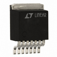
LT1513IR Linear Technology, LT1513IR Datasheet - Page 11

LT1513IR
Manufacturer Part Number
LT1513IR
Description
IC BATT CHRGR CONST/PROG I/V 7DD
Manufacturer
Linear Technology
Datasheet
1.LT1513-2CR.pdf
(16 pages)
Specifications of LT1513IR
Function
Charge Management
Battery Type
All Battery Types
Voltage - Supply
2.7 V ~ 25 V
Operating Temperature
-40°C ~ 125°C
Mounting Type
Surface Mount
Package / Case
TO-263-8, D²Pak (7 leads + Tab), TO-263CA
Lead Free Status / RoHS Status
Contains lead / RoHS non-compliant
Available stocks
Company
Part Number
Manufacturer
Quantity
Price
Company:
Part Number:
LT1513IR
Manufacturer:
LINEARTE
Quantity:
462
Part Number:
LT1513IR#PBF
Manufacturer:
LINEAR/凌特
Quantity:
20 000
Part Number:
LT1513IR#TR
Manufacturer:
LINEAR/凌特
Quantity:
20 000
Part Number:
LT1513IR#TRPBF
Manufacturer:
LINEAR/凌特
Quantity:
20 000
APPLICATIONS
(from the Electrical Characteristics). Amplifier output resis-
tance is modeled with a 330k resistor. The power stage
(modulator section) of the LT1513 is modeled as a transcon-
ductance whose value is 4(V
simplified model of the actual power stage, but it is sufficient
when the unity-gain frequency of the loop is low compared
to the switching frequency. The output filter capacitor model
includes its ESR (R
assigned to the battery model.
Analysis of this loop normally shows an extremely stable
system for all conditions, even with 0 for R5. The one
condition which can cause reduced phase margin is with a
very large battery resistance (>5 ), or with the battery
replaced with a resistive load. The addition of R5 gives good
phase margin even under these unusual conditions. R5
should not be increased above 330 without checking for
two possible problems. The first is instability in the constant
current region (see Constant-Current Mode Loop Stability),
and the second is subharmonic switching where switch duty
cycle varies from cycle to cycle. This duty cycle instability is
caused by excess switching frequency ripple voltage on the
V
filtering effect of C5, but large values of R5 can allow high
ripple on the V
C
pin. Normally this ripple is very low because of the
C
pin. Normal loop analysis does not show this
THIS IS A SIMPLIFIED AC MODEL FOR THE LT1513 IN
CONSTANT-CURRENT MODE. RESISTOR AND CAPACITOR
NUMBERS CORRESPOND TO THOSE USED IN FIGURE 1.
R
C3 IS 3pF FOR A 10 H INDUCTOR. IT SHOULD BE SCALED
PROPORTIONALLY FOR OTHER INDUCTOR VALUES (6pF
FOR 20 H). THE PowerPath IS A TRANSCONDUCTANCE
WHOSE GAIN IS A FUNCTION OF INPUT AND BATTERY
VOLTAGE AS SHOWN.
P
CAP
U
AND C
FB
V
C
R5
330
). A series resistance (R
C5
0.1 F
P
INFORMATION
MODEL THE PHASE DELAY IN THE PowerPath.
U
IN
)/(V
R
1M
R
330k
P
G
IN
**
W
+ V
1500 mho
Figure 7. Constant-Current Small-Signal Model
BAT
g
EA
m
C
3pF
P
V1
). This is a very
–
+
BAT
U
MODULATOR SECTION
) is also
I
P
1.245V
=
4(V1)(V
V
IN
+ V
BAT
THE CURRENT AMPLIFIER HAS A FIXED VOLTAGE GAIN OF 12.
ITS PHASE DELAY IS MODELED WITH R
THE ERROR AMPLIFIER HAS A TRANSCONDUCTANCE OF
1500 mho AND AN INTERNAL OUTPUT SHUNT RESISTANCE OF
330k.
AS SHOWN, THIS LOOP HAS A UNITY-GAIN FREQUENCY OF
ABOUT 27kHz. R5 IS NOT USED IN ALL APPLICATIONS, BUT IT
GIVES BETTER PHASE MARGIN IN CONSTANT VOLTAGE MODE.
IN
100k
)
R
C
10pF
A
A
problem, and indeed small signal loop stability can be
excellent even in the presence of subharmonic switching.
The primary issue with subharmonics is the presence of EMI
at frequencies below 500kHz.
Constant-Current Mode Loop Stability
The LT1513 is normally very stable when operating in con-
stant-current mode (see Figure 7), but there are certain con-
ditions which may create instabilities. The combination of
higher value current sense resistors (low programmed charg-
ing current), higher input voltages, and the addition of a loop
compensation resistor (R5) on the V
stable current mode loop. (A resistor is sometimes added in
series with C5 to improve loop phase margin when the loop
is operating in voltage mode.) Instability results
because loop gain is too high in the 50kHz to 150kHz region
where excess phase occurs in the current sensing amplifier
and the modulator. The I
pole at approximately 150kHz. The modulator section con-
sisting of the current comparator, the power switch and the
magnetics, has a pole at approximately 50kHz when the
coupled inductor value is 10 H. Higher inductance will reduce
the pole frequency proportionally. The design procedure pre-
sented here is to roll off the loop to unity-gain at a frequency
of 25kHz or lower to avoid these excess phase regions.
VOLTAGE
GAIN = 12
I
FBA
–
+
I
FB
A
I
P
AND C
FBA
24
C4
0.22 F
A
LT1513/LT1513-2
R4
.
amplifier (gain of –12.5) has a
R3
0.1
C
pin may create an un-
1513 F07
sn1513 1513fas
11


