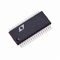
LTC1960CG Linear Technology, LTC1960CG Datasheet - Page 8

LTC1960CG
Manufacturer Part Number
LTC1960CG
Description
IC BATT CHRGR/SELECTR DUAL36SSOP
Manufacturer
Linear Technology
Datasheet
1.LTC1960CGPBF.pdf
(28 pages)
Specifications of LTC1960CG
Function
Charge Management
Voltage - Supply
6 V ~ 28 V
Operating Temperature
0°C ~ 70°C
Mounting Type
Surface Mount
Package / Case
36-SSOP (0.200", 5.30mm Width)
Lead Free Status / RoHS Status
Contains lead / RoHS non-compliant
Available stocks
Company
Part Number
Manufacturer
Quantity
Price
Part Number:
LTC1960CG
Manufacturer:
LINEAR/凌特
Quantity:
20 000
Part Number:
LTC1960CG#PBF
Manufacturer:
LINEAR/凌特
Quantity:
20 000
PIN FUNCTIONS
LTC1960
Input Power Related
SCN (Pin 4/Pin 30): PowerPath Current Sensing Negative
Input. This pin should be connected directly to the “bottom”
(output side) of the sense resistor, R
three PowerPath switch pairs, for detecting short-circuit
current events. Also powers LTC1960 internal circuitry
when all other sources are absent.
SCP (Pin 5/Pin 31): PowerPath Current Sensing Positive
Input. This pin should be connected directly to the “top”
(switch side) of the sense resistor, R
three PowerPath switch pairs, for detecting short-circuit
current events.
GDCO (Pin 6/Pin 32): DCIN Output Switch Gate Drive.
Together with GDCI, this pin drives the gate of the P-channel
switch in series with the DCIN input switch.
GDCI (Pin 7/Pin 33): DCIN Input Switch Gate Drive.
Together with GDCO, this pin drives the gate of the
P-channel switch connected to the DCIN input.
GB1O (Pin 8/Pin 34): BAT1 Output Switch Gate Drive.
Together with GB1I, this pin drives the gate of the P-channel
switch in series with the BAT1 input switch.
GB1I (Pin 9/Pin 35): BAT1 Input Switch Gate Drive.
Together with GB1O, this pin drives the gate of the P-channel
switch connected to the BAT1 input.
GB2O (Pin 10/Pin 36): BAT2 Output Switch Gate Drive.
Together with GB2I, this pin drives the gate of the P-channel
switch in series with the BAT2 input switch.
GB2I (Pin 11/Pin 37): BAT2 Input Switch Gate Drive.
Together with GB2O, this pin drives the gate of the P-channel
switch connected to the BAT2 input.
CLP (Pin 24/Pin 13): The Positive Input to the Supply
Current Limiting Amplifier CL1. The threshold is set at
100mV above the voltage at the DCIN pin. When used
to limit supply current, a filter is needed to filter out the
switching noise.
8
(G/UHF)
SC
SC
, in series with the
, in series with the
Battery Charging Related
V
Resistor Divider Which Provides Battery Voltage Feedback
to the Charger. A capacitor from CSN to V
V
for the voltage loop.
I
the Current Mode PWM. Higher I
higher charging current in normal operation. A capacitor
of at least 0.1µF to GND filters out PWM ripple. Typical
full-scale output current is 30µA. Nominal voltage range
for this pin is 0V to 2.4V.
I
required to filter higher frequency components from the
delta-sigma IDAC.
CSN (Pin 22/Pin 11): Current Amplifier CA1 Input. Con-
nect this to the common output of the charger MUX
switches.
CSP (Pin 23/Pin 12): Current Amplifier CA1 Input. This
pin and the CSN pin measure the voltage across the
sense resistor, R
rent signals required for both peak and average current
mode operation.
COMP1 (Pin 25/Pin 14): The Compensation Node for the
Amplifier CL1. A capacitor is required from this pin to GND
if input current amplifier CL1 is used. At input adapter
current limit, this node rises to 1V. By forcing COMP1 low,
amplifier CL1 will be defeated (no adapter current limit).
COMP1 can source 10µA.
BGATE (Pin 27/Pin 16): Drives the bottom external MOSFET
of the battery charger buck converter.
SW (Pin 30/Pin 19): PWM switch node connected to source
of the top external MOSFET switch. Used as reference for
top gate driver.
BOOST (Pin 31/Pin 20): Supply to Topside Floating Driver.
The bootstrap capacitor is returned to this pin. Voltage
swing at this pin is from a diode drop below V
+ V
TH
SET
SET
SET
CC
(Pin 14/Pin 2): The Control Signal of the Inner Loop of
(Pin 15/Pin 3): A capacitor from I
to GND provide necessary compensation and filtering
(Pin 13/Pin 1): The Tap Point of a Programmable
).
SNS
, to provide the instantaneous cur-
TH
voltage corresponds to
SET
SET
to ground is
CC
and from
to (DCIN
1960fb


