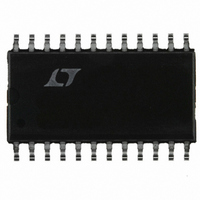
LT1511ISW Linear Technology, LT1511ISW Datasheet - Page 15

LT1511ISW
Manufacturer Part Number
LT1511ISW
Description
IC BATT CHRGR CONST I/V 3A24SOIC
Manufacturer
Linear Technology
Datasheet
1.LT1511CSWPBF.pdf
(16 pages)
Specifications of LT1511ISW
Function
Charge Management
Battery Type
Li-Ion, NiCd, NiMH
Voltage - Supply
6 V ~ 28 V
Operating Temperature
-40°C ~ 85°C
Mounting Type
Surface Mount
Package / Case
24-SOIC (0.300", 7.50mm Width)
Lead Free Status / RoHS Status
Contains lead / RoHS non-compliant
Available stocks
Company
Part Number
Manufacturer
Quantity
Price
Part Number:
LT1511ISW
Manufacturer:
LINEAR/凌特
Quantity:
20 000
Company:
Part Number:
LT1511ISW#PBF
Manufacturer:
TI
Quantity:
696
Part Number:
LT1511ISW#PBF
Manufacturer:
LINEAR/凌特
Quantity:
20 000
Company:
Part Number:
LT1511ISW#TRPBF
Manufacturer:
LT
Quantity:
3 140
Part Number:
LT1511ISW#TRPBF
Manufacturer:
LTNEAR
Quantity:
20 000
APPLICATIONS
off instantly when the input is dead shorted to avoid large
current surges from the battery back through the charger
into the FET. Gate capacitance slows turn-off, so a small
P-channel (Q2) is to discharge the gate capacitance quickly
in the event of an input short. The body diode of Q2 creates
the necessary pumping action to keep the gate of Q1 low
during normal operation. Note that Q1 and Q2 have a V
spec limit of 20V. This restricts V
For low dropout operation with V
Optional Connection of Input Diode and
Current Sense Resistor
The typical application shown in Figure 1 on the first page
of this data sheet shows a single diode to isolate the V
pin from the adapter input. This simple connection may be
unacceptable in situations where the main system power
must be disconnected from both the battery and the
adapter under some conditons. In particular, if the adapter
is disconnected or turned off and it is desired to also
L1
L1
Figure 12b. Modified Input Diode Connection
SW
R
SW
R
S1
PARASITIC
INTERNAL
S1
LT1511
PARASITIC
INTERNAL
DIODE
LT1511
Figure 12a. Standard Connection
DIODE
CLP
CLN
V
CLN
CC
CLP
V
U
CC
+
+
INFORMATION
U
+
+
C
C1
1 F
IN
500
500
C
Information furnished by Linear Technology Corporation is believed to be accurate and reliable.
However, no responsibility is assumed for its use. Linear Technology Corporation makes no represen-
tation that the interconnection of its circuits as described herein will not infringe on existing patent rights.
C1
1 F
R7
R7
IN
IN
IN
D3
to a maximum of 20V.
> 20V consult factory.
W
R
S4
R
D3
S4
D4
ADAPTER
IN
TO
SYSTEM
POWER
1511 F12a
ADAPTER
IN
TO
SYSTEM
POWER
1511 F12b
U
GS
CC
disconnect the system load from the battery, the system
will remain powered through the parasitic diode from the
SW pin to the V
The circuit in Figure 12b allows system power to go to 0V
without drawing battery current by adding an additional
diode, D4. To ensure proper operation, the LT1511 current
sense amplifier inputs (CLP and CLN) were designed to
work above V
inputs are pulled to ground by a powered-down adapter.
Layout Considerations
Switch rise and fall times are under 10ns for maximum
efficiency. To prevent radiation, the catch diode, SW pin
and input bypass capacitor leads should be kept as short
as possible. A ground plane should be used under the
switching circuitry to prevent interplane coupling and to
act as a thermal spreading path. All ground pins should be
connected to expanded traces for low thermal resistance.
The fast-switching high current ground path, including the
switch, catch diode and input capacitor, should be kept
very short. Catch diode and input capacitor should be
close to the chip and terminated to the same point. This
path contains nanosecond rise and fall times with several
amps of current. The other paths contain only DC and/or
200kHz tri-wave and are less critical. Figure 13 indicates
the high speed, high current switching path. Figure 14
shows critical path layout. Contact Linear Technology for
an actual LT1511 circuit PCB layout or Gerber file.
V
IN
C
Figure 13. High Speed Switching Path
IN
CC
and not to draw current from V
CC
CIRCULATING
FREQUENCY
pin.
SWITCH NODE
PATH
HIGH
D1
L1
C
OUT
LT1511
CC
when the
15
BAT
LT1511 • F13
V
BAT


