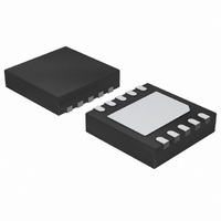
NCP1835MN24T2G ON Semiconductor, NCP1835MN24T2G Datasheet

NCP1835MN24T2G
Specifications of NCP1835MN24T2G
NCP1835MN24T2GOSTR
Available stocks
Related parts for NCP1835MN24T2G
NCP1835MN24T2G Summary of contents
Page 1
NCP1835 Integrated Li-Ion Charger NCP1835 is an integrated linear charger specifically designed to charge 1−cell Li−Ion batteries with a constant current, constant voltage (CCCV) profile. It can charge at currents 1.0 A. Its low input voltage capability, ...
Page 2
4 GND PIN FUNCTION DESCRIPTION Pin Symbol 1 V Input Supply Voltage. Provides power to the charger. This pin should be bypassed with at least a 4.7 mF ceramic CC capacitor to ground. ...
Page 3
V CC Startup, Control & Clamp V2P8 V2P8 VCC Resistor Dividers VREF CFLG FAULT MAXIMUM RATINGS Rating Supply Voltage Status Flag Output Pins Voltage Range for Other Pins Current Out from BAT Pin Thermal Characteristics Thermal Resistance, Junction−to−Air (Note 3) ...
Page 4
ELECTRICAL CHARACTERISTICS are guaranteed over 0°C to 70°C with a supply voltage in the range of 4 6.5 V, unless otherwise noted.) Characteristic V SUPPLY CC Operating Supply Range Rising V Threshold CC Falling V Lockout Threshold CC ...
Page 5
TYPICAL OPERATING CHARACTERISTICS 4.30 4.242 V 4.25 4.20 4.2 V 4. ISEL 4.00 0 0.2 0.4 0 CHARGE CURRENT (A) CHG Figure 3. Regulated Output Voltage vs. ...
Page 6
TYPICAL OPERATING CHARACTERISTICS 3.0 2.5 2.0 1.5 1.0 0.5 0.0 3.7 3.9 4.1 4.3 4.5 4.7 4 INPUT VOLTAGE (V) CC Figure 8. V2P8 Voltage vs. Input Voltage 120 110 100 ...
Page 7
Overview Rechargeable Li−Ion/Polymer batteries are normally charged with a constant current (CC) until the terminal voltage reaches a fixed voltage threshold, at which point a constant voltage (CV) is applied and the current drawn by the battery decays. The charging ...
Page 8
Power Up V > POR N Y POR Initialization Reset Counter Trickle Charge V > SNS 1/8 TIMEOUT? Y Trickle Charge Set FAULT Low Latch Up Charger N EN Toggled? Y ...
Page 9
Trickle Charge RISE V BAT charge I PC CFLG FAULT V2P8 0 Table 1. Charge Status Condition Trickle, Constant Current and Constant Voltage Charge End−of−Charge or Shutdown Mode Timeout Fault, V < 0.35 V ...
Page 10
Charge Status Indicator (CFLG) CFLG is an open−drain output that indicates battery charging or End−of−Charge (EOC) status pulled low when charging in constant current mode and constant voltage mode. It will be forced to a high impedance state ...
Page 11
Input and Output Capacitor Selection A 4 higher value ceramic capacitor is recommended for the input bypass capacitor. For the output capacitor, when there is no battery inserted and the NCP1835 is used as an LDO with 4.2 ...
Page 12
The following Table 3 shows the desired TIMEOUT vs. C sizes. The C is required for proper device TIME TIME operation. Table 3. TIMEOUT vs. C Size TIME C (nF) TIMEOUT (minute) TIME 0.47 1 5.6 8 ...
Page 13
PCB Layout Recommendations The recommended footprint for the 3x3 mm DFN package is included on the Package Dimension page critical that the exposed metal pad is properly soldered to the ground copper area and then connected to a ...
Page 14
Figure 23. Silkscreen Layer Figure 24. Top Layer Figure 25. Bottom Layer http://onsemi.com 14 ...
Page 15
... Test Pin 17 2 Header Pin Pinch = 2.54 mm ORDERING INFORMATION Device Voltage Option NCP1835MN20R2 NCP1835MN20R2G NCP1835MN24T2 NCP1835MN24T2G †For information on tape and reel specifications, including part orientation and tape sizes, please refer to our Tape and Reel Packaging Specifications Brochure, BRD8011/D. Designators ...
Page 16
... Pb−Free strategy and soldering details, please download the ON Semiconductor Soldering and Mounting Techniques Reference Manual, SOLDERRM/D. N. American Technical Support: 800−282−9855 Toll Free USA/Canada Europe, Middle East and Africa Technical Support: Phone: 421 33 790 2910 Japan Customer Focus Center Phone: 81− ...


