TC14433EPG Microchip Technology, TC14433EPG Datasheet - Page 3
TC14433EPG
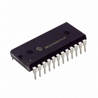
Manufacturer Part Number
TC14433EPG
Description
IC ADC 3 1/2 DIGIT 24DIP
Manufacturer
Microchip Technology
Specifications of TC14433EPG
Display Type
LED
Configuration
7 Segment
Interface
BCD
Digits Or Characters
A/D 3.5 Digits
Current - Supply
1.8mA
Voltage - Supply
4.5 V ~ 8 V
Operating Temperature
-40°C ~ 85°C
Mounting Type
Through Hole
Package / Case
24-DIP (0.600", 15.24mm)
Resolution (bits)
3.5bit
Sampling Rate
25SPS
Input Channel Type
Single Ended
Data Interface
BCD
Supply Current
800µA
Digital Ic Case Style
DIP
No. Of Pins
24
Lead Free Status / RoHS Status
Lead free / RoHS Compliant
Available stocks
Company
Part Number
Manufacturer
Quantity
Price
Company:

Part Number:
TC14433EPG
Manufacturer:
MICROCHIP
Quantity:
1 800
Part Number:
TC14433EPG
Manufacturer:
TOSHIBA/东芝
Quantity:
20 000


1.0
Absolute Maximum Ratings*
Supply Voltage (V
Voltage on Any Pin:
DC Current, Any Pin: ........................................ ±10mA
Power Dissipation (T
Operating Temperature Range ............... 0°C to +70°C
Storage Temperature Range .............. -65°C to +160°C
©
TC14433/A ELECTRICAL SPECIFICATIONS
Electrical Characteristics: V
R
Analog Input
SYE
NL
SOR
ZOR
I
CMRR
Note 1: Accuracy - The accuracy of the meter at full scale is the accuracy of the setting of the reference voltage. Zero is
Symbol
IN
2002 Microchip Technology Inc.
1
Reference to V
= 27kΩ @ V
Plastic PDIP.................................................. 940W
SOIC ............................................................. 940W
Plastic PLCC ................................................. 1.0W
CERDIP ....................................................... 1.45W
2: The LSD stability for 200mV scale is defined as the range that the LSD will occupy 95% of the time.
3: Pin numbers refer to 24-pin PDIP.
ELECTRICAL
CHARACTERISTICS
Rollover Error (Positive) and
Negative Full Scale
Symmetry
Linearity Output Reading
(Note 1)
Stability Output Reading
(Note 2)
Zero Output Reading
Bias Current: Analog Input
Common mode Rejection
recalculated during each conversion cycle. The meaningful specification is linearity. In other words, the deviation from
correct reading for all inputs other than positive full scale and zero is defined as the linearity specification.
REF
Parameter
DD
EE
= 200mV, unless otherwise specified.
A
Reference Input
Analog Ground
– V
.....................-0.5V to (V
≤ 70°C):
EE
) ................... -0.5V to +18V
DD
= +5V, V
-1 count
EE
-0.05
Min
—
—
—
—
—
—
—
-1
= -5V, C
DD
T
A
1
+0.05
+ 0.5)
= +25°C
Typ
±20
±20
±20
—
—
—
—
65
= 0.1µF, (Mylar), C
0
+1 count
+0.05
±100
±100
±100
Max
+1
—
2
3
0
*Stresses above those listed under "Absolute Maximum
Ratings" may cause permanent damage to the device. These
are stress ratings only and functional operation of the device
at these or any other conditions above those indicated in the
operation sections of the specifications is not implied.
Exposure to Absolute Maximum Rating conditions for
extended periods may affect device reliability.
0
= 0.1µF, R
Min
—
—
—
—
—
—
—
—
—
—
T
A
= +25°C
Typ
—
—
—
—
—
—
—
—
—
—
C
= 300kΩ, R
Max
—
—
—
—
—
—
—
—
—
—
1
TC14433/A
Counts 200mV Full Scale
= 470kΩ @ V
Units
%rdg
%rdg
LSD
LSD
LSD
pA
pA
pA
dB
V
V
V
V
V
V
V
V
V
F
IN
REF
REF
X
REF
X
REF
X
X
OC
Test Conditions
= 1.99V,
= 199mV,
= 0V, V
= 1.4V, V
-V
DS21394B-page 3
= 32kHz
REF
= 2V
= 200mV
= 2V
= 200mV
IN
= +V
= 2V,
REF
REF
IN
= 2V
= 2V,
Related parts for TC14433EPG
Image
Part Number
Description
Manufacturer
Datasheet
Request
R

Part Number:
Description:
Manufacturer:
Microchip Technology Inc.
Datasheet:
Part Number:
Description:
Manufacturer:
Microchip Technology Inc.
Datasheet:
Part Number:
Description:
Manufacturer:
Microchip Technology Inc.
Datasheet:
Part Number:
Description:
Manufacturer:
Microchip Technology Inc.
Datasheet:
Part Number:
Description:
Manufacturer:
Microchip Technology Inc.
Datasheet:
Part Number:
Description:
Manufacturer:
Microchip Technology Inc.
Datasheet:
Part Number:
Description:
Manufacturer:
Microchip Technology Inc.
Datasheet:
Part Number:
Description:
Manufacturer:
Microchip Technology Inc.
Datasheet: