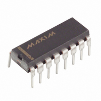
MAX6958AAPE+ Maxim Integrated Products, MAX6958AAPE+ Datasheet - Page 7

MAX6958AAPE+
Manufacturer Part Number
MAX6958AAPE+
Description
IC DRVR DSPL LED 16-DIP
Manufacturer
Maxim Integrated Products
Datasheet
1.MAX6958AAEE.pdf
(19 pages)
Specifications of MAX6958AAPE+
Display Type
LED
Configuration
7 Segment + 2 Annunciators
Interface
SMBus (2-Wire/I²C)
Digits Or Characters
4 Digits
Current - Supply
5.9mA
Voltage - Supply
3 V ~ 5.5 V
Operating Temperature
-40°C ~ 125°C
Mounting Type
Through Hole
Package / Case
16-DIP (0.300", 7.62mm)
Number Of Digits
4
Number Of Segments
36
Low Level Output Current
275 mA
High Level Output Current
30 mA
Operating Supply Voltage
3 V to 5.5 V
Maximum Supply Current
6.7 mA
Maximum Power Dissipation
842 mW
Maximum Operating Temperature
+ 125 C
Mounting Style
Through Hole
Minimum Operating Temperature
- 40 C
Lead Free Status / RoHS Status
Lead free / RoHS Compliant
One data bit is transferred during each clock pulse.
The data on the SDA line must remain stable while SCL
is high (Figure 4).
The acknowledge bit is a clocked 9th bit that the recipi-
ent uses to handshake receipt of each byte of data
(Figure 5). Thus, each byte transferred effectively
requires 9 bits. The master generates the 9th clock
pulse, and the recipient pulls down SDA during the
acknowledge clock pulse, such that the SDA line is sta-
ble low during the high period of the clock pulse. When
the master is transmitting to the MAX6958/MAX6959,
the MAX6958/MAX6959 generate the acknowledge bit
because the MAX6958/MAX6959 are the recipients.
When the MAX6958/MAX6959 are transmitting to the
master, the master generates the acknowledge bit
because the master is the recipient.
The MAX6958/MAX6959 have a 7-bit-long slave
address (Figure 3). The eighth bit following the 7-bit
slave address is the R/W bit. Set the R/W bit low for a
write command and high for a read command.
Figure 3. Slave Address
Figure 4. Bit Transfer
Figure 6. Command Byte Received
SDA
SCL
9-Segment LED Display Drivers with Keyscan
SDA
SCL
DATA STABLE,
DATA VALID
S
MSB
0
COMMAND BYTE IS STORED ON RECEIPT OF STOP CONDITION
_______________________________________________________________________________________
CHANGE OF
DATA ALLOWED
SLAVE ADDRESS
2-Wire Interfaced, 3V to 5.5V, 4-Digit,
1
1
ACKNOWLEDGE FROM
MAX6958/MAX6959
Slave Address
Acknowledge
Bit Transfer
R/W
1
0
A
D15
0
The MAX6958/MAX6959 are available in one of two
possible slave addresses (see Table 2 and Ordering
Information). The first 6 bits (MSBs) of the MAX6958/
MAX6959 slave address are always 011100. Slave
address bit A0 is internally hardwired to either GND in
the MAX695_A_, or V+ in the MAX695_B_. A maximum
of two MAX6958/MAX6959 devices can share a bus.
A write to the MAX6958/MAX6959 comprises the trans-
mission of the MAX6958/MAX6959s’ slave address with
the R/W bit set to zero, followed by at least 1 byte of
information. The first byte of information is the com-
mand byte, which determines the register that stores
the next byte written to the MAX6958/MAX6959. If a
STOP condition is detected after the command byte is
received, the MAX6958/MAX6959 take no further action
(Figure 6) beyond storing the command byte.
Figure 5. Acknowledge
Table 2. MAX6958/MAX6959 Address Map
SLAVE ADDRESS
D14
SCL
SDA
CONDITION
MAX695_A_
MAX695_B_
START
D13
BIT A0
0
COMMAND BYTE
D12
D11
1
LSB
ACKNOWLEDGE FROM
A0
D10
MAX6958/MAX6959 DEVICE ADDRESS
MAX6958/MAX6959
A6
Message Format for Writing
0
0
2
D9
A5
1
1
D8
R/W
NOT ACKNOWLEDGE
A4
1
1
ACKNOWLEDGE
A
A3
8
ACKNOWLEDGMENT
1
1
CLOCK PULSE FOR
P
ACK
A2
0
0
9
A1
0
0
A0
0
1
7


