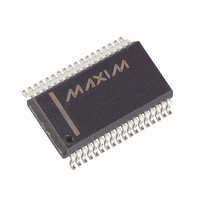
MAX6955AAX+T Maxim Integrated Products, MAX6955AAX+T Datasheet - Page 4

MAX6955AAX+T
Manufacturer Part Number
MAX6955AAX+T
Description
IC DRVR DSPL LED 36-SSOP
Manufacturer
Maxim Integrated Products
Datasheet
1.MAX6955AAX.pdf
(43 pages)
Specifications of MAX6955AAX+T
Display Type
LED
Configuration
7, 14, 16 Segment
Interface
I²C
Current - Supply
22mA
Voltage - Supply
2.7 V ~ 5.5 V
Operating Temperature
-40°C ~ 125°C
Mounting Type
Surface Mount
Package / Case
36-SSOP
Number Of Digits
16
Number Of Segments
128
Low Level Output Current
935 mA
High Level Output Current
55 mA
Operating Supply Voltage
2.7 V to 5.5 V
Maximum Supply Current
30 mA
Maximum Power Dissipation
941 mW
Maximum Operating Temperature
+ 125 C
Mounting Style
SMD/SMT
Minimum Operating Temperature
- 40 C
Lead Free Status / RoHS Status
Lead free / RoHS Compliant
Digits Or Characters
-
Lead Free Status / Rohs Status
Details
2-Wire Interfaced, 2.7V to 5.5V LED Display
Driver with I/O Expander and Key Scan
TIMING CHARACTERISTICS
(Typical Operating Circuit, V+ = 2.7V to 5.5V, T
Note 1: All parameters tested at T
Note 2: Guaranteed by design.
Note 3: A master device must provide a hold time of at least 300ns for the SDA signal (referred to V
Note 4: C
Note 5: I
Note 6: Input filters on the SDA and SCL inputs suppress noise spikes less than 50ns.
4
TIMING CHARACTERISTICS
Serial Clock Frequency
Bus Free Time Between a STOP
and a START Condition
Hold Time (Repeated) START
Condition
Repeated START Condition Setup
Time
STOP Condition Setup Time
Data Hold Time
Data Setup Time
SCL Clock Low Period
SCL Clock High Period
Rise Time of Both SDA and SCL
Signals, Receiving
Fall Time of Both SDA and SCL
Signals, Receiving
Fall Time of SDA Transmitting
Pulse Width of Spike Suppressed
Capacitive Load for Each
Bus Line
_______________________________________________________________________________________
bridge the undefined region of SCL’s falling edge.
SINK
B
PARAMETER
= total capacitance of one bus line in pF. t
≤ 6mA. C
B
= total capacitance of one bus line in pF. t
A
= +25°C. Specifications over temperature are guaranteed by design.
SYMBOL
t
t
t
t
HD
HD,
SU
t
SU
SU:STO
t
t
t
f
t
HIGH
LOW
F
SCL
BUF
t
C
, t
, t
, t
t
t
SP
, t
R
F
t
B
STA
DAT
DAT
STA
X
A
= T
(Note 3)
(Notes 2, 4)
(Notes 2, 4)
(Notes 2, 5)
(Notes 2, 6)
(Note 2)
MIN
R
and t
to T
MAX
F
measured between 0.3V+ and 0.7V+.
, unless otherwise noted.) (Note 1)
CONDITIONS
R
and t
F
measured between 0.3V+ and 0.7V+.
MIN
100
1.3
0.6
0.6
0.6
1.3
0.6
0
IL
- of the SCL signal) in order to
0.1C
0.1C
0.1C
20 +
20 +
20 +
TYP
400
B
B
B
MAX
400
300
300
300
0.9
50
UNITS
kHz
pF
µs
µs
µs
µs
µs
ns
µs
µs
ns
ns
ns
ns


