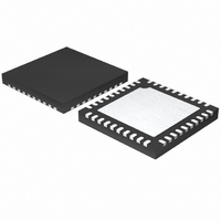
MAX6955ATL+T Maxim Integrated Products, MAX6955ATL+T Datasheet - Page 2

MAX6955ATL+T
Manufacturer Part Number
MAX6955ATL+T
Description
IC DRVR DSPL LED 40-TQFN
Manufacturer
Maxim Integrated Products
Datasheet
1.MAX6955AAX.pdf
(43 pages)
Specifications of MAX6955ATL+T
Display Type
LED
Configuration
7, 14, 16 Segment
Interface
I²C
Current - Supply
22mA
Voltage - Supply
2.7 V ~ 5.5 V
Operating Temperature
-40°C ~ 125°C
Mounting Type
Surface Mount
Package / Case
40-TQFN Exposed Pad
Number Of Digits
16
Number Of Segments
128
Low Level Output Current
935 mA
High Level Output Current
55 mA
Operating Supply Voltage
2.7 V to 5.5 V
Maximum Supply Current
30 mA
Maximum Power Dissipation
2051.3 mW
Maximum Operating Temperature
+ 125 C
Mounting Style
SMD/SMT
Minimum Operating Temperature
- 40 C
Lead Free Status / RoHS Status
Lead free / RoHS Compliant
Digits Or Characters
-
Lead Free Status / Rohs Status
Details
2-Wire Interfaced, 2.7V to 5.5V LED Display
Driver with I/O Expander and Key Scan
ABSOLUTE MAXIMUM RATINGS
Voltage (with Respect to GND)
Current
DC ELECTRICAL CHARACTERISTICS
(Typical Operating Circuit, V+ = 2.7V to 5.5V, T
Stresses beyond those listed under “Absolute Maximum Ratings” may cause permanent damage to the device. These are stress ratings only, and functional
operation of the device at these or any other conditions beyond those indicated in the operational sections of the specifications is not implied. Exposure to
absolute maximum rating conditions for extended periods may affect device reliability.
2
Operating Supply Current
Operating Supply Voltage
Shutdown Supply Current
Master Clock Frequency
Dead Clock Protection Frequency
OSC Internal/External Detection
Threshold
OSC High Time
OSC Low Time
Slow Segment Blink Period
Fast Segment Blink Period
Fast or Slow Segment Blink Duty
Cycle
V+ .........................................................................-0.3V to +6V
SCL, SDA, AD0, AD1 ...........................................-0.3V to +6V
All Other Pins............................................-0.3V to (V+ + 0.3V)
O0–O7 Sink Current ......................................................935mA
O0–O18 Source Current .................................................55mA
SCL, SDA, AD0, AD1, BLINK, OSC, OSC_OUT, ISET ....20mA
P0, P1, P2, P3, P4/IRQ ....................................................40mA
GND .....................................................................................1A
_______________________________________________________________________________________
PARAMETER
f
SLOWBLINK
f
SYMBOL
FASTBLINK
I
V
SHDN
f
f
t
OSC
OSC
t
V+
OSC
CH
I+
CL
A
= T
Shutdown mode, all
digital inputs at V+
or GND
All segments on, all
digits scanned,
intensity set to full,
internal oscillator, no
display or OSC_OUT
load connected
OSC = RC oscillator, R
C
OSC driven externally
OSC = RC oscillator, R
C
OSC = RC oscillator, R
C
SET
SET
SET
MIN
= 22pF, V+ = 3.3V
= 22pF, V+ = 3.3V
= 22pF, V+ = 3.3V
to T
MAX
, unless otherwise noted.) (Note 1)
CONDITIONS
Continuous Power Dissipation (T
Operating Temperature Range
Junction Temperature ......................................................+150°C
Storage Temperature Range .............................-65°C to +150°C
Lead Temperature (soldering, 10s) .................................+300°C
36-Pin SSOP (derate at 11.8mW/°C above +70°C) .....941mW
40-Pin TQFN (derate at 25.6mW/°C above +70°C)....2051.3mW
(T
T
T
T
T
SET
SET
SET
MIN
A
A
A
A
= +25°C
= T
= +25°C
= T
= 56kΩ,
= 56kΩ,
= 56kΩ,
to T
MIN
MIN
MAX
to T
to T
) ...............................................-40°C to +125°C
MAX
MAX
49.5
MIN
2.7
50
50
1
A
= +70°C)
TYP
1.7
0.5
10
22
95
4
1
MAX
50.5
5.5
35
40
30
35
8
UNITS
MHz
kHz
mA
µA
ns
ns
%
V
V
s
s


