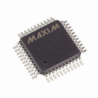
MAX6960AMH+D Maxim Integrated Products, MAX6960AMH+D Datasheet - Page 18

MAX6960AMH+D
Manufacturer Part Number
MAX6960AMH+D
Description
IC DRVR LED 8X8 44-MQFP
Manufacturer
Maxim Integrated Products
Datasheet
1.MAX6963ATH.pdf
(35 pages)
Specifications of MAX6960AMH+D
Display Type
LED
Configuration
8 x 8 (Matrix)
Interface
4-Wire Serial
Digits Or Characters
Any Digit Type
Current - Supply
7.5mA
Voltage - Supply
2.7 V ~ 3.6 V
Operating Temperature
-40°C ~ 125°C
Mounting Type
Surface Mount
Package / Case
44-MQFP, 44-PQFP
Number Of Segments
64
Low Level Output Current
750000 uA
High Level Output Current
48000 uA
Operating Supply Voltage
2.7 V to 3.6 V
Maximum Supply Current
11 mA
Maximum Power Dissipation
1012 mW
Maximum Operating Temperature
+ 125 C
Mounting Style
SMD/SMT
Minimum Operating Temperature
- 40 C
Lead Free Status / RoHS Status
Lead free / RoHS Compliant
The power-up sequence consists of an internal power-on
reset (POR), assertion of the external reset input RST,
and auto-address configuration (see the Local 3-Wire
Interface section). The internal POR resets all control
registers to the default values shown in Table 12.
After RST goes high an internal timer delays execution of
the auto-address configuration for 2
cycles (nominally 250ms at OSC = 4.194MHz) (see the
3-Wire Interface Clock (ADDCLK) section). During this
delay time, the global driver devices register (0x0E),
global driver rows register (0x0F), and global panel con-
figuration register (0x0D) should be written as these
4-Wire Serially Interfaced
8 x 8 Matrix Graphic LED Drivers
Table 15. Global Panel Configuration Register Format
Table 16. Global Panel Configuration—Shutdown Control (S Data Bit D0) Format
Table 17. Global Panel Configuration—Invert Pixels (IP Data Bit D1) Format
Table 18. Global Panel Configuration—Current Plane (DP0, DP1 Data Bit D2, D3) Format
18
Shutdown
Normal operation
Logic 1 in display memory lights the appropriate
LED (normal logic)
Logic 0 in display memory lights the appropriate
LED (invert logic)
______________________________________________________________________________________
Current display plane is P0
Current display plane is P1
Current display plane is P2
Current display plane is P0
Current display plane is P3
Current display plane is P1
Global panel configuration
REGISTER
REGISTER
REGISTER
REGISTER
Initial Power-Up
21
(2,097,152) OSC
CODE (HEX)
CODE (HEX)
CODE (HEX)
CODE (HEX)
ADDRESS
ADDRESS
ADDRESS
ADDRESS
0x0D
0x0D
0x0D
0x0D
0x0D
0x0D
0x0D
0x0D
0x0D
0x0D
0x0D
values are used in the auto-address configuration
sequence (see the Device Configuration section). After
the internal delay time, the auto-addressing configuration
commences and takes a fixed interval of 256 ADDCLK
cycles to complete where the ADDCLK frequency is
OSC/4 (see the 3-Wire Interface Clock (ADDCLK) sec-
tion). After completing the auto-self-addressing of all
possible 256 interconnected devices, all of the
MAX6960s enter shutdown mode.
All registers are capable of write device register opera-
tions during the internal delay interval using the 4-wire
serial interface. Read device register operations are not
allowed during auto-address configuration.
D7
D7
D7
D7
PI
PI
PI
PI
PI
PI
PI
0
1
0
1
D6
D6
D6
D6
C
C
C
C
C
C
C
C
C
C
C
D5
D5
D5
D5
F
F
F
F
F
F
F
F
F
F
F
REGISTER DATA
REGISTER DATA
REGISTER DATA
REGISTER DATA
D4
D4
D4
D4
R
R
R
R
R
R
R
R
R
R
R
DP1
DP1
DP1
DP1
DP1
D3
D3
D3
D3
0
0
1
1
1
1
DP0
DP0
DP0
DP0
DP0
D2
D2
D2
D2
0
1
0
0
1
1
D1
D1
D1
D1
IP
IP
IP
IP
IP
IP
IP
IP
IP
0
1
D0
D0
D0
D0
S
S
S
S
S
S
S
0
1
S
S


