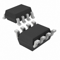
LTC4360CSC8-1#TRPBF Linear Technology, LTC4360CSC8-1#TRPBF Datasheet - Page 7

LTC4360CSC8-1#TRPBF
Manufacturer Part Number
LTC4360CSC8-1#TRPBF
Description
IC CTLR OVP 80V SHUTDOWN SC70-8
Manufacturer
Linear Technology
Type
Overvoltage Protection Controllerr
Datasheet
1.LTC4360CSC8-1TRMPBF.pdf
(14 pages)
Specifications of LTC4360CSC8-1#TRPBF
Applications
General Purpose
Internal Switch(s)
No
Voltage - Supply
2.5 V ~ 5.5 V
Operating Temperature
0°C ~ 70°C
Mounting Type
Surface Mount
Package / Case
8-VSSOP
Lead Free Status / RoHS Status
Lead free / RoHS Compliant
Available stocks
Company
Part Number
Manufacturer
Quantity
Price
APPLICATIONS INFORMATION
The GATE ramp rate is limited to 3V/ms. V
a similar rate which results in an inrush current into the
load capacitor C
The servo loop is compensated by the parasitic capaci-
tance of the external MOSFET. No further compensation
components are normally required. In the case where the
parasitic capacitance is less than 100pF , a 100pF compensa-
tion capacitor between GATE and ground may be required.
An even slower GATE ramp and lower inrush current can
be achieved by connecting an external capacitor, C
GATE to ground. The voltage at GATE then ramps up with a
slope equal to 10µA/C
Overvoltage
When power is first applied, V
(V
ramped up to turn on the MOSFET. If V
5.8V (V
30mA fast pull-down on GATE within 1µs. After an over-
voltage condition, the MOSFET is held off until V
again remains below 5.7V for 130ms.
PWRGD Output
PWRGD is an active low output with a MOSFET pull-
down to ground and a 500k resistive pull-up to OUT. The
PWRGD pin pull-down releases during the low current
sleep mode (invoked by ON high), UVLO or overvolt-
age and the subsequent 130ms start-up delay. After the
start-up delay, GATE starts its slow ramp-up and control
of the PWRGD pull-down passes on to the GATE high
comparator. V
the PWRGD pull-down and V
the pull-down. The PWRGD pull-down is capable of sink-
ing up to 3mA of current allowing it to drive an optional
LED. To interface PWRGD to another I/O rail, connect a
resistor from PWRGD to the I/O rail with a resistance
low enough to override the internal 500k pull-up to OUT.
IN(OV)
I
C
INRUSH
G
=
IN(OV)
I
– ∆V
INRUSH
10µA
= C
), the overvoltage comparator activates the
OV
GATE
OUT
) for more than 130ms before GATE is
OUT
• C
> V
•
OUT
dV
of:
G
GATE(TH)
[V/s]. Choose C
GATE
dt
= C
for more than 65ms asserts
IN
GATE
OUT
must remain below 5.7V
< V
• 3 mA/µF
G
IN
using the formula:
[
GATE(TH)
then rises above
OUT
follows at
]
releases
IN
G
, from
once
Figure 2 details PWRGD behavior for a LTC4360-1 with
1k pull-up to 5V at PWRGD.
ON Input (LTC4360-1)
ON is a CMOS compatible, active low enable input. It
has a default 5µA pull-down to ground. Connect this
pin to ground or leave open to enable normal device
operation. If it is driven high while the external MOSFET
is turned on, GATE is pulled low with a weak pull-down
current (40µA) to turn off the external MOSFET gradually,
minimizing input voltage transients. The LTC4360-1 then
goes into a low current sleep mode, drawing only 1.5µA
at IN. When ON goes back low, the part restarts with a
130ms delay cycle.
GATEP Control (LTC4360-2)
GATEP has a 2M resistive pull-down to ground and a 5.8V
Zener clamp in series with a 200k resistor to IN. It con-
trols the gate of an optional external P-channel MOSFET
to provide negative voltage protection. The 2M resistive
pull-down turns on the MOSFET once V
more than the MOSFET gate threshold voltage. The IN to
GATEP Zener protects the MOSFET from gate overvoltage
by clamping its V
PWRGD
GATE
OUT
ON
IN
V
130ms
FROM UVLO
IN(UVL)
START-UP
LTC4360-1/LTC4360-2
65ms
V
GATE(TH)
V
IN(OV)
Figure 2. PWRGD Behavior
GS
to 5.8V when V
OV
130ms
V
IN(OV)
RESTART
FROM OV
–∆V
65ms
OV
V
GATE(TH)
IN
goes high.
ON
V
GATE(TH)
IN
130ms
RESTART
FROM ON
– V
GATEP
65ms
V
GATE(TH)
436012fa
7
is


