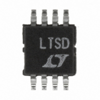
LTC4211IMS8#TRPBF Linear Technology, LTC4211IMS8#TRPBF Datasheet - Page 11

LTC4211IMS8#TRPBF
Manufacturer Part Number
LTC4211IMS8#TRPBF
Description
IC CONTROLLER HOT SWAP 8-MSOP
Manufacturer
Linear Technology
Type
Hot-Swap Controllerr
Datasheet
1.LTC4211IMS8PBF.pdf
(36 pages)
Specifications of LTC4211IMS8#TRPBF
Applications
General Purpose
Internal Switch(s)
No
Voltage - Supply
2.5 V ~ 16.5 V
Operating Temperature
-40°C ~ 85°C
Mounting Type
Surface Mount
Package / Case
8-TSSOP, 8-MSOP (0.118", 3.00mm Width)
Linear Misc Type
Positive Low Voltage
Family Name
LTC4211
Package Type
MSOP
Operating Supply Voltage (min)
2.5V
Operating Supply Voltage (max)
16.5V
Operating Temperature (min)
-40C
Operating Temperature (max)
85C
Operating Temperature Classification
Industrial
Product Depth (mm)
3mm
Product Height (mm)
0.86mm
Product Length (mm)
3mm
Mounting
Surface Mount
Pin Count
8
Lead Free Status / RoHS Status
Lead free / RoHS Compliant
Available stocks
Company
Part Number
Manufacturer
Quantity
Price
BLOCK DIAGRA
PI FU CTIO S
FAULT (Not available on S8/MS8, Pin 10 MS): FAULT is
both an input and an output. Connected to this pin are an
analog comparator (COMP6) and an open-drain N-chan-
nel FET. During normal operation, if COMP6 is driven
below 1.236V, the electronic circuit breaker trips and the
GATE pin pulls low. Typically, a 10k pull-up resistor
connects to the FAULT pin. This allows the LTC4211 to
begin a second timing cycle (V
properly. This also allows the use of the FAULT pin as a
status output. Under normal operating conditions, the
FAULT output is a logic high. Two conditions cause an
active low on FAULT: (1) the LTC4211’s electronic circuit
breaker trips because of an output short circuit (V
MS ONLY
U
FILTER
TIMER
3 (4)
(3)
NOTE 1: SET BY FILTER CAPACITOR FOR MS
PIN NUMBERS FOR S8/MS8 (MS)
10µA
2µA
2µA
U
M6
M5
M4
V
V
20µs DEFAULT FOR MS8, S8
CC
CC
V
V
0.2V
REF
REF
U
+
–
+
–
+
–
COMP3
COMP4
COMP5
t
(8-Lead Package/10-Lead Package)
TIMER
W
NORMAL
NORMAL, RESET
FAULT
FAULT
UVLO
> 1.286) and start-up
V
CC
8 (9)
GLITCH FILTER
(SEE NOTE 1)
+
SLOW
COMP
–
+
–
50mV
OUT
+
2
GLITCH FILTER
SENSE
DELAY
COMP
300ns
FAST
–
=
COMP1
ON
150µs
–
+
–
LOGIC
7 (8)
V
+
REF
150mV
0V) or because of a fast output overcurrent transient
(FAST COMP trips circuit breaker); or (2) V
1.236V. The FAULT output is driven to logic low and is
latched logic low until the ON pin is driven to logic low for
150µs (the t
FILTER (Not available S8/MS8, Pin 3 MS): Overcurrent
Fault Timing Pin and Overvoltage Fault Set pin. With a
capacitor connected from this pin to ground, the SLOW
COMP’s response time can be adjusted. In the S8/MS8
version of the LTC4211, the FILTER pin is not available and
the delay time from overcurrent detect to GATE OFF is fixed
at 20µs.
5 (6)
GLITCH FILTER
FUNCTION OF
OVERDRIVE
–
COMP2
FB
M3
CB
TRIPS
OR UVLO
COMP7
V
+
REF
RESET
–
+
200µA
ON LOW
GATE
0.2V
duration).
6 (7)
REGULATOR
START-UP
CURRENT
V
0.2V
REF
10µA
10µA
V
Z
(TYP) = 12V
CHARGING
CHARGE
PUMP
BG
GATE
POWER BAD
CB TRIPS
Z1
V
CC
COMP6
+
–
Z2
V
Z
LTC4211
(TYP) = 26V
V
M1
M2
REF
4211 BD
FILTER
RESET
1
FAULT
(10)
MS ONLY
GND
4 (5)
11
4211fa
>


