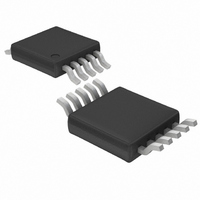
LTC4252-2CMS#TR Linear Technology, LTC4252-2CMS#TR Datasheet - Page 22

LTC4252-2CMS#TR
Manufacturer Part Number
LTC4252-2CMS#TR
Description
IC CNTRLR HOTSWAP NEGVOLT 10MSOP
Manufacturer
Linear Technology
Type
Hot-Swap Controllerr
Specifications of LTC4252-2CMS#TR
Applications
General Purpose
Internal Switch(s)
No
Operating Temperature
0°C ~ 70°C
Mounting Type
Surface Mount
Package / Case
10-TFSOP, 10-MSOP (0.118", 3.00mm Width)
Family Name
LTC4252-2
Package Type
MSOP
Operating Temperature (min)
0C
Operating Temperature (max)
70C
Operating Temperature Classification
Commercial
Product Depth (mm)
3mm
Product Height (mm)
0.86mm
Product Length (mm)
3mm
Mounting
Surface Mount
Pin Count
10
Lead Free Status / RoHS Status
Contains lead / RoHS non-compliant
Lead Free Status / RoHS Status
Contains lead / RoHS non-compliant
Other names
LTC4252-2CMSTR
LTC42522CMSTR
LTC42522CMSTR
Available stocks
Company
Part Number
Manufacturer
Quantity
Price
LTC4252-1/LTC4252-2
LTC4252A-1/LTC4252A-2
APPLICATIONS INFORMATION
At time point 8, the load current falls and the SENSE voltage
drops below V
off and the GATE pin ramps further. At time point 9, the
SENSE voltage drops below V
ends, followed by a 5.8μA discharge cycle (cool off). The
duration between time points 7 and 9 must be shorter than
one circuit breaker delay to avoid a fault time out during
GATE ramp-up. When GATE ramps past the V
old at time point 10, PWRGD pulls low. At time point 11,
GATE reaches its maximum voltage as determined by V
Live Insertion with Short Pin Control of UV/OV
In the example shown in Figure 10, power is delivered
through long connector pins whereas the UV/OV divider
22
(–48RTN) – (–48V)
GND – V
PWRGD
TIMER
SENSE
DRAIN
UV/OV
EE
GATE
V
ACL
OUT
V
OR
SS
IN
(t). The analog current limit loop shuts
1
V
2
IN
V
V
CLEARS V
GATEL
Figure 9. System Power-Up Timing (All Waveforms Are Referenced to V
LKO
CB
LKO
, the fault TIMER cycle
, CHECK UV > V
5.8μA
INITIAL TIMING
GATEH
UVHI
, OV < V
V
thresh-
TMRH
OVLO
ACL
CB
IN
OS
V
+ V
+ V
, GATE < V
TMRL
.
OS
OS
)
)
58μA
3 4 56
TIMER CLEARS V
makes contact through a short pin. This ensures the power
connections are firmly established before the LTC4252 is
activated. At time point 1, the power pins make contact
and V
divider makes contact and its voltage exceeds V
addition, the internal logic checks for OV < V
< V
V
starts and the TIMER capacitor is charged by a 5.8μA
current source pull-up. At time point 3, TIMER reaches the
V
The TIMER capacitor is quickly discharged. At time point
4, the V
GATE < V
GATEL
TMRL
TMRH
GATEL
START-UP
, SENSE < V
GATE
IN
7
. If all conditions are met, an initial timing cycle
58μA
threshold and the initial timing cycle terminates.
TMRL
ramps through V
8
, SENSE < V
DRN
GATEL
9
10 11
TMRL
CB
threshold is reached and the conditions of
, CHECK GATE < V
V
V
V
V
V
, SENSE < V
IN
ACL
CB
DRNCL
DRNL
– V
GATEH
5.8μA
OS
CB
AND TIMER < V
, SS < 20 • V
LKO
GATEL
CB
EE
. At time point 2, the UV/OV
, SENSE < V
)
and SS < 20 • V
TMRL
5.8μA
CB
425212 F09
OS
and TIMER <
OS
OVHI
must be
OS
UVHI
, GATE
425212fc
. In


