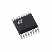
LTC1642CGN#TR Linear Technology, LTC1642CGN#TR Datasheet - Page 7

LTC1642CGN#TR
Manufacturer Part Number
LTC1642CGN#TR
Description
IC CONTROLLER HOTSWAP ADJ 16SSOP
Manufacturer
Linear Technology
Type
Hot-Swap Controllerr
Specifications of LTC1642CGN#TR
Applications
General Purpose, Infiniband™
Internal Switch(s)
No
Voltage - Supply
2.97 V ~ 16.5 V
Operating Temperature
0°C ~ 70°C
Mounting Type
Surface Mount
Package / Case
16-SSOP (0.150", 3.90mm Width)
Lead Free Status / RoHS Status
Contains lead / RoHS non-compliant
Available stocks
Company
Part Number
Manufacturer
Quantity
Price
OV (Pin 9): Overvoltage Input. When the voltage on OV
exceeds its trip point the GATE pin is pulled low immedi-
ately and the CRWBR timer starts. If OV remains above its
trip point (minus 3mV of hysteresis) long enough for
CRWBR to reach its trip point, then the part turns off until
reset by pulsing the ON pin low. Otherwise, the GATE pin
begins ramping up one RST TMR timing cycle after OV
goes below its trip point. Ground the OV pin to disable
overvoltage protection.
COMPOUT (Pin 10): Uncommitted Comparator’s Open
Drain Output.
COMP
ing Input.
COMP
Input.
REF (Pin 13): Reference Voltage Output. The 1.22V ±1%
reference should be bypassed with a 0.1µF compensation
capacitor. For V
GATE (Pin 14): Gate Drive for the External N-Channel
MOSFET. An internal charge pump provides at least 4.5V
of gate drive and sources 25µA. The pin requires an
external series RC network to ground to compensate the
current limit loop and to limit the ramp rate. A resistor of
100Ω is also recommended in series with the MOSFET
PI FU CTIO S
U
+
–
(Pin 11): Uncommitted Comparator’s Noninvert-
(Pin 12): Uncommitted Comparator’s Inverting
U
CC
= 5V it can source 1mA.
U
gate to suppress high frequency oscillations. GATE is
immediately pulled to ground when the overvoltage com-
parator trips or the input supply is below the undervoltage
lockout trip point. During current limit the GATE voltage is
adjusted to maintain constant load current until the circuit
breaker timer trips. At that point GATE is pulled to ground
until the chip is reset. Clamp the GATE pin with an 18V
zener diode (IN4705) to ground if the supply is 8V
or higher.
SENSE (Pin 15): Current Sense Input. To use the current
limit place a sense resistor in the supply path between V
and SENSE. When the drop across the resistor exceeds a
threshold voltage, the GATE pin is adjusted to maintain a
constant load current and the circuit breaker timer is
started. A foldback feature reduces the current limit as the
voltage at FB approaches ground. Short SENSE to V
disable the current limiting.
V
voltage lockout circuit holds the GATE pin at ground until
V
regulator protects the chip from V
voltages up to 33V. In this case the GATE pin voltage will
usually be low but this is not guaranteed; use the OV pin
to ensure that the pass device is off. The V
provides a high side connection to the SENSE resistor.
CC
CC
exceeds 2.73V. If V
(Pin 16): Positive Supply Voltage. An internal under-
CC
exceeds 16.5V an internal shunt
CC
LTC1642
and SENSE pin
CC
pin also
CC
1642fb
7
CC
to


