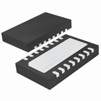
LTC4217CDHC#TRPBF Linear Technology, LTC4217CDHC#TRPBF Datasheet - Page 14

LTC4217CDHC#TRPBF
Manufacturer Part Number
LTC4217CDHC#TRPBF
Description
IC CTRLR HOT SWAP 2A 16-DFN
Manufacturer
Linear Technology
Type
Hot-Swap Switchr
Datasheet
1.LTC4217IFEPBF.pdf
(18 pages)
Specifications of LTC4217CDHC#TRPBF
Applications
General Purpose
Internal Switch(s)
Yes
Current Limit
2.0A
Voltage - Supply
2.9 V ~ 26.5 V
Operating Temperature
0°C ~ 70°C
Mounting Type
Surface Mount
Package / Case
16-WFDFN Exposed Pad
Linear Misc Type
Positive Low Voltage
Package Type
DFN EP
Operating Supply Voltage (min)
2.9V
Operating Temperature (min)
0C
Operating Temperature (max)
70C
Operating Temperature Classification
Commercial
Product Depth (mm)
3mm
Product Length (mm)
5mm
Mounting
Surface Mount
Pin Count
16
Lead Free Status / RoHS Status
Lead free / RoHS Compliant
Available stocks
Company
Part Number
Manufacturer
Quantity
Price
APPLICATIONS INFORMATION
LTC4217
invoked by tying the TIMER pin to INTV
timeout the FLT pin needs to pull-down on the UV pin to
restart the power-up sequence.
Since the default values for overvoltage, undervoltage and
power good thresholds for the 12V fixed version match
the requirements, no external components are required
for the UV, OV and FB pins.
The final schematic in Figure 6 results in very few external
components. The pull-up resistor, R1, connects to the
PG pin while the 20k (R2) converts the I
voltage at a ratio:
In addition there is a 0.1µF bypass (C1) on the INTV
Layout Considerations
In Hot Swap applications where load currents can be 2A,
narrow PCB tracks exhibit more resistance than wider tracks
and operate at elevated temperatures. The minimum trace
width for 1oz copper foil is 0.02" per amp to make sure
the trace stays at a reasonable temperature. Using 0.03"
per amp or wider is recommended. Note that 1oz copper
exhibits a sheet resistance of about 0.5mΩ/square. Small
resistances add up quickly in high current applications.
14
V
IMON
V
DD
Figure 7. Recommended Layout
= 50[µA/A] • 20k • I
HEAT SINK
C
VIA TO
SINK
OUT
= 1[V/A] • I
GND
OUT
CC
MON
4217 F07
. After the 2ms
OUT
current to a
3.3V
CC
pin.
There are two V
that connect to the sense resistor and MOSFET. The PCB
layout should be balanced and symmetrical to each V
pin to balance current in the MOSFET bond wires. Figure 7
shows a recommended layout for the LTC4217.
Although the MOSFET is self protected from overtem-
perature, it is recommended to solder the backside of the
package to a copper trace to provide a good heat sink. Note
that the backside is connected to the SENSE pin and can-
not be soldered to the ground plane. During normal loads
the power dissipated in the MOSFET is as high as 0.23W.
A 10mm × 10mm area of 1oz copper should be sufficient.
This area of copper can be divided in many layers.
It is also important to put C1, the bypass capacitor for
the INTV
and GND.
Additional Applications
The LTC4217 has a wide operating range from 2.9V to 26.5V.
The UV, OV and PG thresholds are set with few resistors.
All other functions are independent of supply voltage.
Figure 8 shows a 3.3V application with a UV threshold of
2.87V, an OV threshold of 3.77V and a PG threshold of
3.05V. The last page includes a 24V application with a UV
threshold of 19.9V, an OV threshold of 26.3V and a PG
threshold of 20.75V.
Figure 8. 3.3V, 1.5A Card Resident Application
17.4k
3.16k
CC
10k
R1
R2
R3
0.1µF
pin as close as possible between the INTV
C
T
DD
pins on opposite sides of the package
V
UV
FLT
OV
TIMER
INTV
DD
LTC4217FE
CC
GND
I
OUT
MON
PG
FB
3.3V
R6
10k
R
20k
14.7k
MON
10k
R4
R5
+
C
100µF
ADC
L
V
3.3V
1.5A
OUT
4217 F08
4217fd
DD
CC


