LTC4253AIUF-ADJ#TRPBF Linear Technology, LTC4253AIUF-ADJ#TRPBF Datasheet
LTC4253AIUF-ADJ#TRPBF
Specifications of LTC4253AIUF-ADJ#TRPBF
Available stocks


Related parts for LTC4253AIUF-ADJ#TRPBF


LTC4253AIUF-ADJ#TRPBF Summary of contents
Page 1
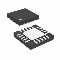
... The LTC4253A-ADJ is available in 20-pin SSOP and 20-pin (4mm × 4mm) QFN packages. , LTC and LT are registered trademarks of Linear Technology Corporation. Hot Swap is a trademark of Linear Technology Corporation. All other trademarks are the property of their respective owners. Patent pending. + ...
Page 2
... (2mA to 30mA UVL = OV = OVL = 4V Coming Out of UVLO (Rising ≤ V ≤ RESET (Sinking TOP VIEW ORDER PART NUMBER LTC4253ACUF-ADJ LTC4253AIUF-ADJ SQTIMER 15 14 TIMER 21 13 UVL OVL UF PART MARKING 253AJ UF PACKAGE = 125°C, θ = 37°C/W JA MUST BE SOLDERED TO PCB EE http://www.linear.com/leadfree/ MIN TYP ● ...
Page 3
ELECTRICAL CHARACTERISTICS temperature range, otherwise specifications are at T SYMBOL PARAMETER I SEL Input Current SEL V Circuit Breaker Current Limit Voltage CB V Analog Current Limit Voltage x% ACL V Circuit Breaker Current Limit Voltage CB V Fast Current ...
Page 4
LTC4253A-ADJ ELECTRICAL CHARACTERISTICS temperature range, otherwise specifications are at T SYMBOL PARAMETER I SQTIMER Pin Current SQTMR V DRAIN Pin Voltage Low Threshold DRNL I DRAIN Leakage Current DRNL V DRAIN Pin Clamp Voltage DRNCL V PWRGD1, PWRGD2, PWRGD3 Signals ...
Page 5
W U TYPICAL PERFOR A CE CHARACTERISTICS and SEL SEL 200 I = 2mA 25°C A 160 I EN 120 SEL ...
Page 6
LTC4253A-ADJ W U TYPICAL PERFOR A CE CHARACTERISTICS V vs Temperature GATEH 3 2mA UV/UVL/OV/OVL = 4V 3 – V GATEH IN GATE 3.2 3.0 2.8 2.6 2.4 2.2 2.0 –50 – ...
Page 7
W U TYPICAL PERFOR A CE CHARACTERISTICS ∆I /∆I vs Temperature TMRACC DRN 9 2mA IN 8.8 8.6 8.4 8.2 8.0 7.8 7.6 7.4 7.2 7.0 50 125 –50 – 100 TEMPERATURE (°C) 4253A G22 ...
Page 8
LTC4253A-ADJ CTIO S (SSOP/QFN) EN2 (Pin 1/Pin 18): Power Good Status Output Two Enable. This is a TTL compatible input that is used to control PWRGD2 and PWRGD3 outputs. When EN2 is driven low, both ...
Page 9
CTIO S (SSOP/QFN) restart after a current limit fault. During GATE start-up, a second comparator detects GATE within 2. before power good sequencing starts. DRAIN (Pin 12/Pin 9): Drain Sense Input. Connecting an ...
Page 10
LTC4253A-ADJ W BLOCK DIAGRA 50µA PWRGD1 SQTIMER DELAY V EE EN2 V IN 120µA 50µ PWRGD2 SQTIMER V EE EN3 V IN 120µA 50µ PWRGD3 SQTIMER V EE OVL 5.09V OVIN OV ...
Page 11
U OPERATIO Hot Circuit Insertion When circuit boards are inserted into a live backplane, the supply bypass capacitors can draw huge transient cur- rents from the power bus as they charge. The flow of current damages the connector pins and ...
Page 12
LTC4253A-ADJ U OPERATIO If RESET < 0.8V occurs after the LTC4253A-ADJ comes out of UVLO (interlock condition 1) and undervoltage (interlock condition 2), GATE and SS are released without an initial TIMER cycle once the other interlock conditions are met ...
Page 13
U OPERATIO comparator with a threshold of 200mV detects overshoot and pulls GATE low much harder and hence much faster than the weaker current limit loop. The V limit loop then takes over, and servos the current as previously described. ...
Page 14
LTC4253A-ADJ U U APPLICATIO S I FOR ATIO SHUNT REGULATOR A fast responding regulator shunts the LTC4253A-ADJ V pin. Power is derived from –48RTN by an external current limiting resistor. The shunt regulator clamps 1µF decoupling ...
Page 15
U U APPLICATIO S I FOR ATIO Figure 2b shows the implementation of the overvoltage function of the Typical Application. During UVLO, OVD is forced high so OVL is multiplexed to OVIN. At time point 1, the part exits UVLO ...
Page 16
LTC4253A-ADJ U U APPLICATIO S I FOR ATIO more noise immunity is desired, add a 1nF to 10nF filter capacitor from UVL UV/OV OPERATION An undervoltage condition detected by the UV comparator immediately shuts down the ...
Page 17
U U APPLICATIO S I FOR ATIO external MOSFET off. To handle this situation, the TIMER discharges C slowly with a 5µA pull-down whenever the T SENSE voltage is less than 50mV. Therefore any intermit- tent overload with V < ...
Page 18
LTC4253A-ADJ U U APPLICATIO S I FOR ATIO When V (t) exceeds V , the ACL amplifier exits ACL SENSE current limit mode and releases its pull-down on GATE • from Equation ...
Page 19
U U APPLICATIO S I FOR ATIO SENSE exceeds 50mV, the CB comparator activates the 200µA TIMER pull-up. At 60mV the ACL amplifier servos the MOSFET current, and at 200mV the FCL comparator abruptly pulls GATE low in an attempt ...
Page 20
LTC4253A-ADJ U U APPLICATIO S I FOR ATIO MOSFET selection is a 3-step process by assuming the absense of soft-start capacitor. First, R then the time required to charge the load capacitance is determined. This timing, along with the maximum ...
Page 21
U U APPLICATIO S I FOR ATIO Actual board evaluation showed that C appropriate. The ratio (R • gauge as large ratios may result in the time-out period expiring prematurely. This gauge is determined ...
Page 22
LTC4253A-ADJ U U APPLICATIO S I FOR ATIO TIMING WAVEFORMS System Power-Up Figure 8 details the timing waveforms for a typical power- up sequence in the case where a board is already installed in the backplane and system power is ...
Page 23
U U APPLICATIO S I FOR ATIO all conditions are met, initial timing starts and the TIMER capacitor is charged by a 5µA current source pull-up. At time point 3, TIMER reaches the V TMRH initial timing cycle terminates. The ...
Page 24
LTC4253A-ADJ U U APPLICATIO S I FOR ATIO point A, setting off the second SQTIMER ramp-up. PWRGD2 pulls low at time point D when EN2 is high and PWRGD1 is low for more than one t . PWRGD3 pulls low ...
Page 25
U U APPLICATIO S I FOR ATIO UVL DROPS BELOW V UVLO UV CLEARS UVL UVLO UVHI TIMER GATE V GATEL SS SENSE DRAIN PWRGD1 PWRGD2 PWRGD3 SQTIMER EN2 EN3 Figure 10. Undervoltage Timing ...
Page 26
LTC4253A-ADJ U U APPLICATIO S I FOR ATIO OV OVERSHOOTS OVHI OVL OV TIMER GATE V GATEL 20 • (V ACL 20 • SENSE Figure 11. Overvoltage Timing (All Waveforms are Referenced to V ...
Page 27
U U APPLICATIO S I FOR ATIO TMRH 200µ • I DRN 5µA TIMER GATE SS V ACL V CB SENSE V OUT DRAIN PWRGD1 CB FAULT (12a) Momentary Circuit Breaker Fault Figure 12. Circuit ...
Page 28
LTC4253A-ADJ U U APPLICATIO S I FOR ATIO 4253a-adjf ...
Page 29
U U APPLICATIO S I FOR ATIO TMRH 200µ • I DRN TIMER GATE SS SENSE V OUT DRAIN PWRGD1 (14a) Analog Current Limit Fault Figure 14. Current Limit Behavior (All Waveforms are Referenced ...
Page 30
LTC4253A-ADJ U U APPLICATIO S I FOR ATIO reflected that ramps up smoothly from near SENSE zero. V does not show a large kink as in Figure 15b SENSE when V (t) already has a substantial offset ...
Page 31
... SHADED AREA IS ONLY A REFERENCE FOR PIN 1 LOCATION ON THE TOP AND BOTTOM OF PACKAGE Information furnished by Linear Technology Corporation is believed to be accurate and reliable. However, no responsibility is assumed for its use. Linear Technology Corporation makes no represen- tation that the interconnection of its circuits as described herein will not infringe on existing patent rights Package 20-Lead Plastic SSOP (Narrow ...
Page 32
... The short-circuit EE reduces as the V voltage increases S OUT is shorted to 71V. OUT C2 POWER R9 100µF MODULE 1 100k POWER C3 MODULE 2 EN POWER MODULE R10 3k V OUT † FMMT493 LT/TP 0805 500 • PRINTED IN USA © LINEAR TECHNOLOGY CORPORATION 2005 POWER MODULE 4 EN 4253 F17 4253a-adjf ...