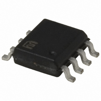
MIC2594-2BM Micrel Inc, MIC2594-2BM Datasheet - Page 18

MIC2594-2BM
Manufacturer Part Number
MIC2594-2BM
Description
IC CTRLR HOT SWAP NEG HV 8-SOIC
Manufacturer
Micrel Inc
Type
Hot-Swap Controllerr
Datasheet
1.MIC2588-1YM_TR.pdf
(21 pages)
Specifications of MIC2594-2BM
Applications
General Purpose
Internal Switch(s)
No
Voltage - Supply
-19 V ~ -80 V
Operating Temperature
-40°C ~ 85°C
Mounting Type
Surface Mount
Package / Case
8-SOIC (0.154", 3.90mm Width)
Lead Free Status / RoHS Status
Contains lead / RoHS non-compliant
Available stocks
Company
Part Number
Manufacturer
Quantity
Price
PCB Layout Considerations
4-Wire Kelvin Sensing
Because of the low value typically required for the sense
resistor, special care must be used to measure accurately
the voltage drop across it. Specifically, the measurement
technique across each R
sensing. This is simply a means of making sure that any
voltage drops in the power traces connecting to the resistors
are not picked up by the signal conductors measuring the
voltages across the sense resistors.
Figure 8 illustrates how to implement 4-wire Kelvin sensing.
As the figure shows, all the high current in the circuit (from
V
MOSFET) flows directly through the power PCB traces
and R
sampled in such a way that the high currents through the
power traces will not introduce any parasitic voltage drops
in the sense leads. It is recommended to connect the hot
swap controller’s sense leads directly to the sense resistor’s
metalized contact pads.
Other Layout Considerations
Figure 9 is a suggested PCB layout diagram for the MIC2588/
MIC2594. Many hot swap applications will require load currents
of several amperes. Therefore, the power (V
trace widths (W) need to be wide enough to allow the current
September 2005
MIC2588/MIC2594
EE
Figure 9. Recommended PCB Layout for Sense Resistor, Power MOSFET, Overvoltage/Undervoltage Resistive
through R
SENSE
. The voltage drop resulting across R
SENSE
, and then to the source of the output
bottom side
Return (VDD)
Via to the
Via to the
Return (VDD)
plane
SENSE
- DRAWING IS NOT TO SCALE-
*See Table 1 for part numbers and vendors
^R1 placed on bottom side
Power Plane -------- (red)
Ground Plane ------- (black)
Trace width (W) guidelines and additional information given in
"PCB Layout Recommendations" section of the datasheet
Via to the
plane
W
R3
must employ 4-wire Kelvin
^R1
from the Load
Current Flow
D1
C1
Divider Network, and Timer Capacitors
GROUND
R2
PAD
*SENSE RESISTOR
EE
/PWRGD
OV
UV
VEE
MIC2588-2BM
(WSR-2 or
WSL2512)
and Return)
SENSE
SENSE
DRAIN
GATE
VDD
is
18
power (VEE output)
to flow while the rise in temperature for a given copper plate
(e.g., 1oz. or 2oz.) is kept to a maximum of 10°C to 25°C.
The return (or power ground) trace should be the same width
as the positive voltage power traces (input/load) and isolated
from any ground and signal planes so that the controller’s
power is common mode. Also, these traces should be as
short as possible in order to minimize the IR drops between
the input and the load.
Finally, the use of plated-through vias will be necessary to
make circuit connections to the power, ground and signal
planes of multi-layer PCBs.
C3
PCB Track Width:
Figure 8. 4-Wire Kelvin Sense Connections for R
0.03" per Ampere
Via to the
using 1oz Cu
plane
R4
*POWER MOSFET
Current Flow
to the Load
(TO-263)
R
Power Trace
From V
to MIC2588/MIC2594 V
FDBK
C
FDBK
EE
ground plane
Via to the
power (VEE output)
Signal Trace
Note: Each SENSE lead trace shall be
balanced for best performance with equal
length/equal aspect ratio.
Via to the
plane
EE
W
Pin
R
SENSE
W
contact pads
R
metalized
SENSE
Signal Trace
to MIC2588/MIC2594 SENSE Pin
To MOSFET Source
M9999-083005
Power Trace
SENSE
Micrel


