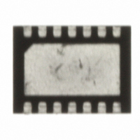
ZXLD1320DCATC Diodes Zetex, ZXLD1320DCATC Datasheet - Page 10

ZXLD1320DCATC
Manufacturer Part Number
ZXLD1320DCATC
Description
IC LED DRVR WHITE BCKLGT 14-TDFN
Manufacturer
Diodes Zetex
Type
Backlight, White LEDr
Datasheet
1.ZXLD1320DCATC.pdf
(18 pages)
Specifications of ZXLD1320DCATC
Topology
PWM, Step-Down (Buck)
Number Of Outputs
1
Internal Driver
Yes
Type - Primary
Automotive
Type - Secondary
High Brightness LED (HBLED)
Frequency
600kHz
Voltage - Supply
4 V ~ 18 V
Mounting Type
Surface Mount
Package / Case
14-TDFN
Operating Temperature
-40°C ~ 125°C
Current - Output / Channel
1.5A
Internal Switch(s)
Yes
Efficiency
85%
Lead Free Status / RoHS Status
Lead free / RoHS Compliant
Voltage - Output
-
Other names
ZXLD1320DCATR
ZXLD1320
ADJ pin
The ADJ pin is connected to the internal 500mV reference (VREF) via a 100k resistor. This biases
the ADJ pin to the reference voltage and defines nominal 100% LED current.
The ADJ pin can be overdriven with an external dc voltage between 50mV and 500mV to reduce
the LED current proportionally between 10% and 100% of the nominal value.
LED current can also be adjusted by applying a low frequency PWM signal to the ADJ pin to turn
the device On and Off. This will produce an average output current proportional to the duty cycle
of the control signal.
The device can be shut down by shorting the ADJ pin to ground, or pulling it to a voltage below
28mV with a suitable open collector NPN or open drain NMOS transistor. In the shutdown state,
most of the circuitry inside the device is switched off and residual quiescent current will be
typically 12µA.
POK output
The POK output comprises a switching transistor driven from the output of the re-triggerable
'500µs monostable'. Operation is such that the POK output remains high during normal operation
(monostable triggered), but switches low if the main switch transistor stays on for more than
500µs (monostable timed out). This output is designed to interface with a microcontroller input
to indicate a fault or out of range condition. It can also be used to drive an indicator LED.
Thermal control of LED current
The 'Thermal compensation current' circuit produces a sourcing current (Itc) which is zero for
voltages above 75mV on TADJ and increases to 100µA when TADJ falls to 50mV. This current is
summed into the control node and subtracted from the demand current, causing LED current to
reduce from 100% down to zero over this input range. The potential divider, consisting of a fixed
resistor Rt and an NTC Thermistor Rth between VREF and ground, defines the voltage on TADJ
and sets the threshold temperature. Further details are given in the application notes.
The Thermal Control feature can be disabled by leaving the TADJ pin floating, or by connecting
it to VREF.
Over-temperature shutdown
The ZXLD1320 incorporates an over-temperature shutdown circuit to protect the device against
damage caused by excess die temperature, resulting from excessive power dissipation in the
switch. The output of the 'Over-temp Shutdown' circuit will go high when the die temperature
exceeds 150°C (nominal). This will turn off the drive to the switch during normal operation.
Operation will resume when the device has cooled to a safe level.
Issue 1 - January 2008
10
www.zetex.com
© Zetex Semiconductors plc 2008


