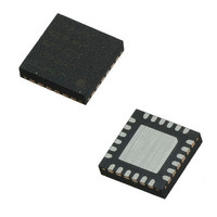
BD6583MUV-AE2 Rohm Semiconductor, BD6583MUV-AE2 Datasheet - Page 4

BD6583MUV-AE2
Manufacturer Part Number
BD6583MUV-AE2
Description
IC LED DRIVER WHIT BCKLGT 24VQFN
Manufacturer
Rohm Semiconductor
Type
Backlight, White LEDr
Specifications of BD6583MUV-AE2
Topology
PWM, Step-Up (Boost)
Number Of Outputs
6
Internal Driver
Yes
Type - Primary
Backlight
Type - Secondary
White LED
Frequency
800kHz ~ 1.2MHz
Voltage - Supply
2.7 V ~ 22 V
Voltage - Output
43V
Mounting Type
Surface Mount
Package / Case
24-VQFN
Operating Temperature
-30°C ~ 85°C
Current - Output / Channel
25mA
Internal Switch(s)
Yes
Lead Free Status / RoHS Status
Lead free / RoHS Compliant
Efficiency
-
Other names
BD6583MUV-AE2TR
BD6583MUV-ATR
BD6583MUV-ATR
BD6583MUV-E2
BD6583MUV-ATR
BD6583MUV-ATR
BD6583MUV-E2
Available stocks
Company
Part Number
Manufacturer
Quantity
Price
Company:
Part Number:
BD6583MUV-AE2
Manufacturer:
ROHM
Quantity:
10 000
Part Number:
BD6583MUV-AE2
Manufacturer:
ROHM/罗姆
Quantity:
20 000
(1) Absolute Maximum Ratings
(2) Power supply and GND line
(3) GND voltage
(4) Short circuit between terminals and erroneous mounting
(5) Operation in strong electromagnetic field
(6) Input terminals
(7) External capacitor
(8) Thermal shutdown circuit (TSD)
(9) Thermal design
(10) DC/DC converter
Cautions on use
An excess in the absolute maximum ratings, such as supply voltage, temperature range of operating conditions,
etc., can break down devices, thus making impossible to identify breaking mode such as a short circuit or an open
circuit. If any special mode exceeding the absolute maximum ratings is assumed, consideration should be given to
take physical safety measures including the use of fuses, etc.
Design PCB pattern to provide low impedance for the wiring between the power supply and the GND lines. Pay
attention to the interference by common impedance of layout pattern when there are plural power supplies
and GND lines. Especially, when there are GND pattern for small signal and GND pattern for large current
included the external circuits, please separate each GND pattern. Furthermore, for all power supply terminals to
ICs, mount a capacitor between the power supply and the GND terminal. At the same time, in order to use a
capacitor, thoroughly check to be sure the characteristics of the capacitor to be used present no problem including
the occurrence of capacity dropout at a low temperature, thus determining the constant.
Make setting of the potential of the GND terminal so that it will be maintained at the minimum in any operating state.
Furthermore, check to be sure no terminals are at a potential lower than the GND voltage including an actual
electric transient.
In order to mount ICs on a set PCB, pay thorough attention to the direction and offset of the ICs. Erroneous
mounting can break down the ICs. Furthermore, if a short circuit occurs due to foreign matters entering
between terminals or between the terminal and the power supply or the GND terminal, the ICs can break
down.
Be noted that using ICs in the strong electromagnetic field can malfunction them.
In terms of the construction of IC, parasitic elements are inevitably formed in relation to potential. The operation of
the parasitic element can cause interference with circuit operation, thus resulting in a malfunction and then
breakdown of the input terminal. Therefore, pay thorough attention not to handle the input terminals, such as to
apply to the input terminals a voltage lower than the GND respectively, so that any parasitic element will operate.
Furthermore, do not apply a voltage to the input terminals when no power supply voltage is applied to the IC. In
addition, even if the power supply voltage is applied, apply to the input terminals a voltage lower than the power
supply voltage or within the guaranteed value of electrical characteristics. And, as the unused input terminals may
make unstable state occur in the internal circuit, please connect them to I/O GND.
In order to use a ceramic capacitor as the external capacitor, determine the constant with consideration given to a
degradation in the nominal capacitance due to DC bias and changes in the capacitance due to temperature, etc.
When junction temperatures become 175°C (typ) or higher, the thermal shutdown circuit operates and turns a
switch OFF. The thermal shutdown circuit, which is aimed at isolating the LSI from thermal runaway as much
as possible, is not aimed at the protection or guarantee of the LSI. Therefore, do not continuously use the
LSI with this circuit operating or use the LSI assuming its operation.
Perform thermal design in which there are adequate margins by taking into account the permissible
dissipation (Pd) in actual states of use.
Please select the low DCR inductors to decrease power loss for DC/DC converter.
Rev.A
4/4


