CAT4016Y-T2 ON Semiconductor, CAT4016Y-T2 Datasheet - Page 8
CAT4016Y-T2
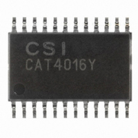
Manufacturer Part Number
CAT4016Y-T2
Description
IC LED DRIVER LINEAR 24-TSSOP
Manufacturer
ON Semiconductor
Type
Linear (Serial Interface)r
Datasheet
1.CAT4016VSR-T2.pdf
(14 pages)
Specifications of CAT4016Y-T2
Constant Current
Yes
Topology
PWM
Number Of Outputs
16
Internal Driver
Yes
Type - Primary
General Purpose
Frequency
25MHz
Voltage - Supply
3 V ~ 5.5 V
Voltage - Output
0.4 V ~ 5.5 V
Mounting Type
Surface Mount
Package / Case
24-TSSOP
Operating Temperature
-40°C ~ 85°C
Current - Output / Channel
80mA
Internal Switch(s)
No
Number Of Digits
16
Number Of Segments
16
High Level Output Current
150 mA
Operating Supply Voltage
3 V to 5.5 V
Maximum Supply Current
100 mA
Maximum Operating Temperature
+ 85 C
Mounting Style
SMD/SMT
Minimum Operating Temperature
- 40 C
Lead Free Status / RoHS Status
Lead free / RoHS Compliant
Efficiency
-
Lead Free Status / Rohs Status
Lead free / RoHS Compliant
Other names
CAT4016Y-T2TR
Available stocks
Company
Part Number
Manufacturer
Quantity
Price
Company:

Part Number:
CAT4016Y-T2
Manufacturer:
ON
Quantity:
2 400
Part Number:
CAT4016Y-T2
Manufacturer:
CSI
Quantity:
20 000


Pin Function
GND is the ground reference pin for the device. This pin
must be connected to the ground plane on the PCB.
SIN is the serial data input. Data is loaded into the internal
register on each rising edge of CLK.
CLK is the serial clock input. On each rising CLK edge, data
is transferred from SIN to the internal 16−bit serial shift
register.
LATCH is the latch data input. On the rising edge of
LATCH, data is loaded from the 16−bit serial shift register
into the output register latch. On the falling edge, this data
is latched in the output register and isolated from the state of
the serial shift register.
LED1 – LED16 are the LED current sink channels. These
pins are connected to the LED cathodes. The current sinks
drive the LEDs with a current equal to 50 times RSET pin
current. For the LED sink to operate correctly, the voltage on
the LED pin must be above 0.4 V.
Table 5. PIN DESCRIPTION
TAB (TQFN package only)
LED1−LED16
LATCH
BLANK
SOUT
Name
RSET
GND
VDD
CLK
SIN
Ground
Serial data input pin
Serial clock input pin
Latch serial data to output registers
LED channel 1 to 16 cathode terminals
Enable / disable all channels
Serial data output pin.
LED current set pin
Positive supply Voltage
Connect to GND on the PCB
http://onsemi.com
8
BLANK is the LED channel enable and disable input pin.
When low, LEDs are enabled according to the output latch
register content. When high, all LEDs are off, while
preserving the data in the output latch register.
SOUT is the serial data output of the 16−bit serial shift
register. This pin is used to cascade several devices on the
serial bus. The SOUT pin is then connected to the SIN input
of the next device on the serial bus to cascade.
RSET is the LED current setting pin. A resistor is connected
between this pin and ground. Each LED channel current is
set to 50 times the current pulled out of the pin. The RSET
pin voltage is regulated to 1.2 V.
VDD is the positive supply pin voltage for the entire device.
A small 1 mF ceramic is recommended close to pin.
Function
Related parts for CAT4016Y-T2
Image
Part Number
Description
Manufacturer
Datasheet
Request
R

Part Number:
Description:
CONTACT BLK,AUX,FRNT,1NO+1NC
Manufacturer:
ABB
Datasheet:
Part Number:
Description:
CONTACT BLK,AUX,FRNT,1NO+1NC
Manufacturer:
ABB
Datasheet:
Part Number:
Description:
CONTACT BLK,AUX,FRNT,1NO+1NC
Manufacturer:
ABB
Datasheet:

Part Number:
Description:
CAT4 RJ45 MODULAR JACK, 8POS, 2 PORT
Manufacturer:
Tyco Electronics
Datasheet:

Part Number:
Description:
CAT4 RJ45 MODULAR JACK, 8POS, 4 PORT
Manufacturer:
Tyco Electronics
Datasheet:

Part Number:
Description:
CAT4 RJ45 MODULAR JACK, 8POS, 5 PORT
Manufacturer:
TE Connectivity
Datasheet:

Part Number:
Description:
CAT4 RJ45 MODULAR JACK, 8POS, 3 PORT
Manufacturer:
TE Connectivity
Datasheet:

Part Number:
Description:
CAT4 RJ45 MODULAR JACK, 8POS, 8 PORT
Manufacturer:
TE Connectivity
Datasheet:


Part Number:
Description:
ON Semiconductor [VOLTAGE REGULATOR]
Manufacturer:
ON Semiconductor
Datasheet:
Part Number:
Description:
357-036-542-201 CARDEDGE 36POS DL .156 BLK LOPRO
Manufacturer:
ON Semiconductor
Datasheet:
Part Number:
Description:
357-036-542-201 CARDEDGE 36POS DL .156 BLK LOPRO
Manufacturer:
ON Semiconductor
Datasheet:
Part Number:
Description:
357-036-542-201 CARDEDGE 36POS DL .156 BLK LOPRO
Manufacturer:
ON Semiconductor
Datasheet:
Part Number:
Description:
357-036-542-201 CARDEDGE 36POS DL .156 BLK LOPRO
Manufacturer:
ON Semiconductor
Datasheet:
Part Number:
Description:
357-036-542-201 CARDEDGE 36POS DL .156 BLK LOPRO
Manufacturer:
ON Semiconductor
Datasheet: