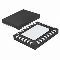
LT3743IUFD#PBF Linear Technology, LT3743IUFD#PBF Datasheet - Page 9

LT3743IUFD#PBF
Manufacturer Part Number
LT3743IUFD#PBF
Description
IC LED DRVR HP CONST CURR 28QFN
Manufacturer
Linear Technology
Type
High Power, Constant Currentr
Datasheet
1.LT3743EUFDPBF.pdf
(28 pages)
Specifications of LT3743IUFD#PBF
Topology
High Side, Low Side, PWM, Step-Down (Buck)
Number Of Outputs
1
Internal Driver
No
Type - Primary
General Purpose
Type - Secondary
RGB
Frequency
200kHz ~ 1MHz
Voltage - Supply
6 V ~ 36 V
Mounting Type
Surface Mount
Package / Case
28-QFN
Operating Temperature
-40°C ~ 125°C
Internal Switch(s)
Yes
Efficiency
92%
Led Driver Application
Lighting
No. Of Outputs
1
Output Current
20A
Output Voltage
40V
Input Voltage
6V To 36V
Dimming Control Type
PWM
Operating Temperature Range
-40°C To +125°C
Rohs Compliant
Yes
Lead Free Status / RoHS Status
Lead free / RoHS Compliant
Voltage - Output
-
Current - Output / Channel
-
Available stocks
Company
Part Number
Manufacturer
Quantity
Price
PIN FUNCTIONS
GND (Pins 1, 5, 9, 20, 21, Exposed Pad Pin 29/Pins 2, 7,
11, 22, 27, Exposed Pad Pin 29): Ground. The exposed
pad must be soldered to the PCB.
EN/UVLO (Pin 2/Pin 4): Enable Pin. The EN/UVLO pin
acts as an enable pin and turns on the internal current
bias core and subregulators at 1.55V. The pin does
not have any pull-up or pull-down, requiring a voltage
bias for normal part operation. Full shutdown occurs at
approximately 0.5V.
V
0.5mA Drive.
CTRL_T (Pin 4/Pin 6): The thermal control input to reduce
the regulated current level for both current levels (CTRL_L
and CTRL_H).
CTRL_H (Pin 6/Pin 8): The CTRL_H pin sets the high level
regulated output current and overcurrent. The maximum
input voltage is internally clamped to 1.5V. The overcurrent
set point is equal to the high level regulated current level
set by the CTRL_H pin with an additional 23mV offset
between the SENSE
CTRL_L (Pin 7/Pin 9): The CTRL_L pin sets the low level
regulated output current. It is not recommended that the
CTRL_L voltage be higher than the CTRL_H voltage.
SS (Pin 8/Pin 10): Soft-Start Pin. Place an external capaci-
tor to ground to limit the regulated current during start-up
conditions. The SS pin has a 5.5μA charging current. This
pin controls both of the regulated inputs determined by
CTRL_L and CTRL_H.
FB (Pin 10/Pin 12): Feedback Pin for Overvoltage Protec-
tion. The feedback voltage is 1V. Overvoltage/Open LED
is sensed through the FB pin. When the feedback voltage
exceeds 1.3V, the overvoltage lockout prevents switching
and connects both output capacitors to discharge the
inductor current.
SENSE
the average current mode loop error amplifi er. This pin is
connected to the external current sense resistor, R
voltage drop between SENSE
the voltage drop across an internal resistor produces the
input voltages to the current regulation loop.
REF
(Pin 3/Pin 5): Buffered 2V Reference Capable of
+
(Pin 11/Pin 13): SENSE
+
and SENSE
(QFN/TSSOP)
+
and SENSE
+
–
is the inverting input of
pins.
–
referenced to
S
. The
SENSE
of the average current mode loop error amplifi er. The refer-
ence current, based on CTRL_L or CTRL_H fl ows out of the
pin to the output (LED) side of the sense resistor, R
VCL (Pin 13/Pin 15): VCL provides the necessary compen-
sation for the average current loop stability during low level
current regulation. Typical compensation values are 15k to
80k for the resistor and 2nF to 10nF for the capacitor.
VCH (Pin 14/Pin 16): VCH provides the necessary com-
pensation for the average current loop stability during
high level current regulation. Typical compensation values
are 15k to 80k for the resistor and 2nF to 10nF for the
capacitor.
RT (Pin 15/Pin 17): A resistor to ground sets the switching
frequency between 200kHz and 1MHz. When using the
SYNC function, set the frequency to be 20% lower than
the SYNC pulse frequency. This pin is current limited to
60μA. Do not leave this pin open.
SYNC (Pin 16/Pin 18): Frequency Synchronization Pin.
This pin allows the switching frequency to be synchronized
to an external clock. The R
operate the internal clock at 20% slower than the SYNC
pulse frequency. The synchronization range is 240kHz to
1.2MHz. This pin should be grounded when not in use.
CTRL_SEL (Pin 17/Pin 19): The CTRL_SEL pin selects
between the high current control, CTRL_H and the low
current control, CTRL_L. When high, the VCH pin is
connected to the error amp output and the PWMGH gate
signal is high. When low, the VCL pin is connected to the
error amp output and the PWMGL gate signal is high. This
pin is used for current level dimming of the LED. This pin
should be grounded when not in use.
PWM (Pin 18/Pin 20): The input pin for PWM dimming
of the LED. When low, all switching is terminated and the
output caps are disconnected. This pin should be pulled
to V
PWMGH (Pin 19/Pin 21): The PWMGH output pin drives
the gate of an external FET to connect one of the switching
regulator output capacitors to the load. The driver pull-up
impedance is 3.2Ω and pull-down impedance is 1.75Ω.
CC_INT
–
(Pin 12/Pin 14): SENSE
when not in use.
T
resistor should be chosen to
–
is the noninverting input
LT3743
S
3743fb
.
9


