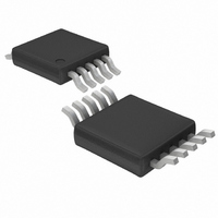
LTC3202EMS Linear Technology, LTC3202EMS Datasheet - Page 8

LTC3202EMS
Manufacturer Part Number
LTC3202EMS
Description
IC LED DRVR WHITE BCKLGT 10-MSOP
Manufacturer
Linear Technology
Type
Backlight, White LEDr
Datasheet
1.LTC3202EDDPBF.pdf
(12 pages)
Specifications of LTC3202EMS
Topology
PWM, Switched Capacitor (Charge Pump)
Number Of Outputs
1
Internal Driver
Yes
Type - Primary
Backlight
Type - Secondary
White LED
Frequency
1.5MHz
Voltage - Supply
2.7 V ~ 4.5 V
Mounting Type
Surface Mount
Package / Case
10-MSOP, Micro10™, 10-uMAX, 10-uSOP
Operating Temperature
-40°C ~ 85°C
Current - Output / Channel
125mA
Internal Switch(s)
Yes
Lead Free Status / RoHS Status
Contains lead / RoHS non-compliant
Voltage - Output
-
Efficiency
-
Available stocks
Company
Part Number
Manufacturer
Quantity
Price
Company:
Part Number:
LTC3202EMS
Manufacturer:
LT
Quantity:
10 469
Part Number:
LTC3202EMS
Manufacturer:
LINEAR/凌特
Quantity:
20 000
Company:
Part Number:
LTC3202EMS#TR
Manufacturer:
ROHM
Quantity:
4 186
Part Number:
LTC3202EMS#TRPBF
Manufacturer:
LTNEAR
Quantity:
20 000
LTC3202
OPERATIO
R
switching term, 1/(2f
tances and the nonoverlap period of the switching circuit.
However, for a given R
will be directly proportional to the advantage voltage
1.5V
Consider the example of driving white LEDs from a
3.1V supply. If the LED forward voltage is 3.8V and the
0.6V V
1.5V – 3.8V – 0.6V or only 250mV. However if the input
voltage is raised to 3.2V the advantage voltage jumps to
400mV—a 60% improvement in available strength! Note
that a similar improvement in advantage voltage can be
achieved by operating the LTC3202 at a lower voltage
setting such as the 0.4V setting.
V
The style and value of capacitors used with the LTC3202
determine several important parameters such as regulator
control loop stability, output ripple, charge pump strength
and minimum start-up time.
To reduce noise and ripple, it is recommended that low
equivalent series resistance (ESR) ceramic capacitors be
used for both C
capacitors are not recommended because of their high ESR.
The value of C
ripple for a given load current. Increasing the size of C
will reduce the output ripple at the expense of higher
minimum turn-on time and higher start-up current. The
peak-to-peak output ripple is approximately given by the
expression:
Where f
cally 1.5MHz) and C
capacitor.
Both the style and value of the output capacitor can
significantly affect the stability of the LTC3202. As shown
8
IN
OL
V
, V
RIPPLEP P
is dependent on a number of factors including the
IN
OUT
FB
– V
OSC
setting is used, the advantage voltage is 3.1V •
Capacitor Selection
OUT
is the LTC3202’s oscillator frequency (typi-
. This voltage can typically be quite small.
OUT
IN
U
3
directly controls the amount of output
f
and C
OSC
OUT
I
OSC
OL
OUT
•
, the amount of current available
C
OUT
is the output charge storage
C
OUT
FLY
. Tantalum and aluminum
), internal switch resis-
OUT
in the block diagram, the LTC3202 uses a control loop to
adjust the strength of the charge pump to match the
current required at the output. The error signal of this loop
is stored directly on the output charge storage capacitor.
The charge storage capacitor also serves to form the
dominant pole for the control loop. To prevent ringing or
instability, it is important for the output capacitor to
maintain at least 0.6 F of capacitance over all conditions.
Likewise, excessive ESR on the output capacitor will tend
to degrade the loop stability of the LTC3202. The closed-
loop output resistance of the LTC3202 is designed to be
0.35 . For a 100mA load current change, the feedback
voltage will change by about 35mV. If the output capacitor
has 0.35
response will cease to roll-off in a simple one-pole fashion
and poor load transient response or instability could
result. Multilayer ceramic chip capacitors typically have
exceptional ESR performance and combined with a tight
board layout should yield very good stability and load
transient performance.
As the value of C
the value of C
input pin (V
relatively constant while the charge pump is on either the
input charging phase or the output charging phase but will
drop to zero during the clock nonoverlap times. Since the
nonoverlap time is small (~25ns) these missing “notches”
will result in only a small perturbation on the input power
supply line. Note that a higher ESR capacitor such as
tantalum will have higher input noise due to the input
current change times the ESR. Therefore ceramic capaci-
tors are again recommended for their exceptional ESR
performance.
Further input noise reduction can be achieved by powering
the LTC3202 through a very small series inductor as
shown in Figure 5. A 10nH inductor will reject the fast
current notches, thereby presenting a nearly constant
current load to the input power supply. For economy the
10nH inductor can be fabricated on the PC board with
about 1cm (0.4") of PC board trace.
IN
or more of ESR the closed-loop frequency
IN
). The input current to the LTC3202 will be
controls the amount of ripple present at the
OUT
controls the amount of output ripple,
3202fa


