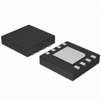
NCV3066MNTXG ON Semiconductor, NCV3066MNTXG Datasheet - Page 2

NCV3066MNTXG
Manufacturer Part Number
NCV3066MNTXG
Description
IC LED DRIVER HIGH BRIGHT 8-DFN
Manufacturer
ON Semiconductor
Type
HBLED Driverr
Datasheet
1.NCP3066DR2G.pdf
(20 pages)
Specifications of NCV3066MNTXG
Constant Current
Yes
Topology
PWM, Step-Down (Buck), Step-Up (Boost)
Number Of Outputs
1
Internal Driver
Yes
Type - Primary
Automotive
Type - Secondary
High Brightness LED (HBLED)
Frequency
100kHz ~ 250kHz
Voltage - Supply
3 V ~ 40 V
Mounting Type
Surface Mount
Package / Case
8-TFDFN Exposed Pad
Operating Temperature
-40°C ~ 125°C
Current - Output / Channel
1.5A
Internal Switch(s)
Yes
Output Current
1.5 A
Input Voltage
3 V to 40 V
Switching Frequency
250 KHz
Mounting Style
SMD/SMT
Lead Free Status / RoHS Status
Lead free / RoHS Compliant
Voltage - Output
-
Efficiency
-
Lead Free Status / Rohs Status
Lead free / RoHS Compliant
Available stocks
Company
Part Number
Manufacturer
Quantity
Price
Company:
Part Number:
NCV3066MNTXG
Manufacturer:
ON Semiconductor
Quantity:
2 900
Part Number:
NCV3066MNTXG
Manufacturer:
ON/安森美
Quantity:
20 000
PIN DESCRIPTION
PDIP8
Comparator Inverting Input
Timing Capacitor
Switch Collector
1
2
3
4
5
6
7
8
Switch Emitter
Pin No.
4, EP Flag
GND
DFN8
1
2
3
5
6
7
8
Figure 2. Pin Connections
I
pk
ON/OFF
Sense
V
CC
SOIC−8/PDIP−8
2
3
4
1
Comparator Inverting Input
(Top View)
8
7
6
5
Timing Capacitor
Switch Collector
Switch Emitter
Pin Name
I
pk
ON/OFF
GND
Comparator
8
7
6
5
V
Sense
CC
ON/OFF
Bias
−
+
0.2 V
ON/OFF
I
V
Comparator
Inverting
Input
pk
CC
Figure 4. Block Diagram
Sense
http://onsemi.com
Comparator
S
R
S
R
Internal Darlington switch collector.
Internal Darlington switch emitter.
Timing Capacitor to control the switching frequency.
Ground pin for all internal circuits.
Inverting input pin of internal comparator.
Voltage Supply
Peak Current Sense Input to monitor the voltage drop across an external
resistor to limit the peak current through the circuit.
ON/OFF Pin. To disable the device, this input should be pulled below
0.8 V. If the pin is left floating, it will be disabled.
+
Q
−
Q
2
Reference
Regulator
Oscillator
TSD
0.235V
Timing Capacitor
Switch Collector
NOTE:
Switch Emitter
EP Flag must be tied to GND Pin 4 on PCB
Figure 3. Pin Connections
GND
Description
CT
Ç Ç Ç Ç
Ç Ç
Ç Ç
1
2
3
4
(Top View)
EP Flag
Switch Collector
Switch Emitter
Timing Capacitor
GND
DFN8
Ç Ç
Ç
Ç
ON/OFF
I
V
Comparator
Inverting
Input
pk
CC
Sense


