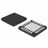
NCP5680MUTXG ON Semiconductor, NCP5680MUTXG Datasheet - Page 4

NCP5680MUTXG
Manufacturer Part Number
NCP5680MUTXG
Description
IC LED DRIVER WHT HI EFF 24-UQFN
Manufacturer
ON Semiconductor
Type
Photo Flash LED (I²C Interface)r
Datasheet
1.NCP5680MUTXG.pdf
(27 pages)
Specifications of NCP5680MUTXG
Topology
Switched Capacitor (Charge Pump)
Number Of Outputs
2
Internal Driver
No
Type - Primary
Flash/Torch
Type - Secondary
White LED
Frequency
850kHz ~ 1.15MHz
Voltage - Supply
2.7 V ~ 5.5 V
Voltage - Output
4.5 V ~ 5.3 V
Mounting Type
Surface Mount
Package / Case
24-UFQFN Exposed Pad, 24-UFQFN
Operating Temperature
-40°C ~ 85°C
Current - Output / Channel
400mA
Internal Switch(s)
Yes
Lead Free Status / RoHS Status
Lead free / RoHS Compliant
Efficiency
-
Lead Free Status / Rohs Status
Details
Available stocks
Company
Part Number
Manufacturer
Quantity
Price
Company:
Part Number:
NCP5680MUTXG
Manufacturer:
ON Semiconductor
Quantity:
2 050
PIN DESCRIPTIONS
1. Using low ESR ceramic capacitor, X5R type, is mandatory to optimize the Charge Pump efficiency and to reduce the EMI. Care must be
2. Total DC/DC output current is limited to 500 mA
Pin
1
2
3
4
5
6
7
8
9
observed to prevent large influence of the ceramic capacitor DC bias: using 10 V rated capacitor, 0805 or 0603 size, is recommended.
PHSEN
TRIGFL
Name
Vgs2
Vds2
VSD
SCL
SDA
NTC
Is2
OUTPUT,
OUTPUT,
ANALOG
ANALOG
ANALOG
ANALOG
DIGITAL
DIGITAL
DIGITAL
POWER
POWER
INPUT,
INPUT,
INPUT,
INPUT,
INPUT,
INPUT,
INPUT,
Type
This pin provides the 2.5 V Photo sense bias voltage. The bias voltage is connected when either
a flash sequence has been selected, or the ENPH bit, in the CONFIG0 register, is set High. The
output current is limited to 1 mA. The same pin is used to synchronize the charge pump operation
by an external digital signal (see Figure 6).
This pin fulfills two functions:
PHOTO SENSE FUNCTION: the pin is connected to the external photo transistor. The operating
voltage is limited in the 0 V to 1.7 V range. The voltage signal developed across that pin and
ground during a flash sequence is compared with the PHREF voltage (encoded in one I2C data
byte) to stop the flash pulse when the illumination is completed. This function is activated by the
ENPH bit of the CONFIG0 register:
pulse width, but is automatically limited by the Time out.
and the amount of light reflected by the scene, but limited by the Time Out.
The PHREF reference is setup by the external MCU and stored into a built−in register through
the I2C lines.
CHARGE PUMP SYNC: the charge pump is de−activated when an external DC voltage (V
in the 2.1 V to 2.5 V range, is applied to the PHSEN pin, whatever be the status of the photo
sense transistor. The PHSEN resumes to the normal operation when the V
nected from the pin.
This pin carries the I2C clock to control the DC/DC converter and to set up the output current.
The SCL clock is associated with the SDA signal.
This pin carries the data provided by the I2C protocol. A normal I2C sequence must send the I2C
address plus a pair of SDA byte to properly program the embedded registers.
This pin supports the digital signal coming from an external peripheral to trig the flash pulse. The
duration of this positive pulse drives the LED, the photo sense being a way to accurately control
the illumination of the scene. The TRIGFL signal is independent from the I2C interface, assuming
the supercap has been properly charged to the appropriate voltage prior to launch the flash trig-
ger. The built−in time out makes sure the flash duration does not extend the programmed limit
(ranging from 2 ms to 200 ms).
In addition, an internal pull−down resistor (100 kW typical) makes sure the pin is not floating when
it is not connected to an external network.
This pin monitors the external Negative Temperature Coefficient resistor. A programmable con-
stant current is provided by the pin (10 mA typical) and the internal structure compares the result-
ing voltage against the programmed limit, the result being a stop of the power current when V
is lower than Vlimit.
This pin, associated to Vgs2 and the Vout pin, returns the sense voltage, developed across the
external shunt resistor, to the LED#2 current control loop. Care must be observed to avoid noise,
stray capacitance and parasitic ohmic element between the shunt resistor and this point to min-
imize the parasitic pulses on the LED output current.
This pin controls the gate of the external NMOS device and the LED is activated when the bit
BLED1=1 in the Select Register byte. Care must be observed to minimize the routing between
this pin and the gate of the external device. Similarly, the PCB track shall be designed to sustain
the relative high current pulse flowing into the Ciss during the normal operation. The built−in
driver structure is capable to control 10 A rated NMOS device with Ciss up to 2500 pF.
This pin fulfils two functions:
− support the I−LED when the Torch mode is activated. In this case, the Gate drive Vgs1 and
Vgs2 signals are deactivated. The internal current mirror, programmed by the I2C port, limits the
ILED1 to 100 mA maximum.
− sense the Drain voltage across the external NMOS #2 to detect the overload condition: see
Table 2.
ENPH = 0 ³ the Photo sense is not activated, the flash time depends solely upon the TRIGFL
ENPH = 1 ³ the Photo sense is activated, the flash time depends upon the TRIGFL duration
http://onsemi.com
4
Description
MSK
voltage is discon-
MSK
NTC
),


