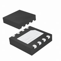
MAX1599ETA+T Maxim Integrated Products, MAX1599ETA+T Datasheet - Page 8

MAX1599ETA+T
Manufacturer Part Number
MAX1599ETA+T
Description
IC LED DRIVR WHITE BCKLGT 8-TDFN
Manufacturer
Maxim Integrated Products
Type
Backlight, White LEDr
Datasheet
1.MAX1561ETAT.pdf
(10 pages)
Specifications of MAX1599ETA+T
Constant Current
Yes
Topology
PWM, Step-Up (Boost)
Number Of Outputs
1
Internal Driver
Yes
Type - Primary
Backlight
Type - Secondary
White LED
Frequency
400kHz ~ 600kHz
Voltage - Supply
2.6 V ~ 5.5 V
Voltage - Output
26V
Mounting Type
Surface Mount
Package / Case
8-TDFN Exposed Pad
Operating Temperature
-40°C ~ 85°C
Current - Output / Channel
700mA
Internal Switch(s)
Yes
Efficiency
87%
Number Of Segments
6
Operating Supply Voltage
2.6 V to 5.5 V
Maximum Power Dissipation
1950 mW
Maximum Operating Temperature
+ 85 C
Mounting Style
SMD/SMT
Minimum Operating Temperature
- 40 C
Lead Free Status / RoHS Status
Lead free / RoHS Compliant
input and output ripple, but at the expense of size and
higher cost. C
trols soft-start. Connect a 0.1µF capacitor from COMP
to GND. For stable operation, C
10 times C
Inductor values range from 10µH to 47µH. A 22µH
(47µH for the MAX1599) inductor optimizes the efficien-
cy for most applications while maintaining low 15mV
input ripple. With input voltages near 5V, a larger value
of inductance can be more efficient. To prevent core
saturation, ensure that the inductor-saturation current
rating exceeds the peak inductor current for the appli-
cation. Calculate the peak inductor current with the fol-
lowing formula:
The MAX1561/MAX1599s’ high switching frequency
demands a high-speed rectification diode (D1) for opti-
mum efficiency. A Schottky diode is recommended due
to its fast recovery time and low forward-voltage drop.
Ensure that the diode’s average and peak current rating
exceed the average output current and peak inductor
current. In addition, the diode’s reverse breakdown volt-
age must exceed V
calculated from:
High-Efficiency, 26V Step-Up Converters
for Two to Six White LEDs
8
_______________________________________________________________________________________
I
PEAK
=
COMP
V
OUT MAX
I
DIODE RMS
COMP
0 8
(
.
.
(
×
OUT
)
V
×
stabilizes the converter and con-
IN MIN
Schottky Diode Selection
)
. The RMS diode current can be
(
I
LED MAX
≅
)
(
I
OUT
)
Inductor Selection
×
+
OUT
I
PEAK
V
IN MIN
(
must not exceed
2
)
×
×
L
0 8
.
µ
s
P-P
Due to fast switching waveforms and high-current
paths, careful PC board layout is required. An evalua-
tion kit (MAX1561EVKIT) is available to speed design.
Order MAX1599 samples separately.
When laying out a board, minimize trace lengths between
the IC and R
capacitor, and the output capacitor. Keep traces short,
direct, and wide. Keep noisy traces, such as the LX node
trace, away from CS. The IN bypass capacitor (C
should be placed as close to the IC as possible. PGND
and GND should be connected directly to the exposed
paddle underneath the IC. The ground connections of
C
The traces from IN to the inductor and from the Schottky
diode to the LEDs may be longer.
TRANSISTOR COUNT: 2895
PROCESS: BiCMOS
IN
and C
OUT
SENSE
should be as close together as possible.
Applications Information
, the inductor, the diode, the input
Chip Information
PC Board Layout
IN
)


