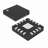
MAX7302ATE+T Maxim Integrated Products, MAX7302ATE+T Datasheet - Page 23

MAX7302ATE+T
Manufacturer Part Number
MAX7302ATE+T
Description
IC LED DRIVER LINEAR 16-TQFN
Manufacturer
Maxim Integrated Products
Type
Linear (I²C Interface)r
Datasheet
1.MAX7302AEE.pdf
(30 pages)
Specifications of MAX7302ATE+T
Topology
Open Drain, PWM
Number Of Outputs
9
Internal Driver
Yes
Type - Primary
Backlight, LED Blinker
Type - Secondary
White LED
Frequency
1MHz
Voltage - Supply
1.62 V ~ 3.6 V
Mounting Type
Surface Mount
Package / Case
16-TQFN Exposed Pad
Operating Temperature
-40°C ~ 125°C
Current - Output / Channel
25mA
Internal Switch(s)
Yes
Lead Free Status / RoHS Status
Lead free / RoHS Compliant
Voltage - Output
-
Efficiency
-
Lead Free Status / Rohs Status
Details
The acknowledge bit is a clocked 9th bit that the recipi-
ent uses to handshake receipt of each byte of data (see
Figure 13). Thus, each effectively transferred byte
requires 9 bits. The master generates the 9th clock
pulse, and the recipient pulls down SDA during the
acknowledge clock pulse, such that the SDA line is sta-
ble low during the high period of the clock pulse. When
the master is transmitting to the MAX7302, the MAX7302
generates the acknowledge bit because the MAX7302
is the recipient. When the MAX7302 is transmitting to the
master, the master generates the acknowledge bit
because the master is the recipient.
The MAX7302 has a 7-bit long slave address (Figure
14). The 8th bit following the 7-bit slave address is the
R/W bit. Set R/W bit low for a write command and high
for a read command.
The first 5 bits of the MAX7302 slave address (A6–A2)
are always 1, 0, 0, 1, and 1. Slave address bit A1, A0 is
selected by the address input AD0. AD0 can be con-
nected to GND, V
four possible slave addresses (see Table 5), and there-
fore, a maximum of four MAX7302 devices can be con-
trolled independently from the same interface.
Figure 13. Acknowledge
Figure 14. Slave Address
Figure 15. Register Address Received
TRANSMITTER
Level-Translating GPIO and LED Driver with CLA
RECEIVER
SDA BY
SDA BY
SDA
SCL
SCL
CONDITION
START
S
MSB
1
S
DD
______________________________________________________________________________________
1
, SDA, or SCL. The MAX7302 has
0
2
SLAVE ADDRESS
FOR ACKNOWLEDGE
ACKNOWLEDGE FROM MAX7302
The Slave Address
0
CLOCK PULSE
Acknowledge
8
R/W
1
SMBus/I
9
0
A
1
D15
A write to the MAX7302 comprises the transmission of the
MAX7302’s slave address with the R/W bit set to zero, fol-
lowed by at least 1 byte of information (see Figure 16).
The first byte of information is the command byte. The
command byte determines which register of the
MAX7302 is to be written to by the next byte, if received.
If a STOP condition is detected after the command byte is
received, the MAX7302 takes no further action beyond
storing the command byte (see Figure 15).
Any bytes received after the command byte are data
bytes. The first data byte goes into the internal register of
the MAX7302 selected by the command byte (see Figure
16). If multiple data bytes are transmitted before a STOP
condition is detected, these bytes are generally stored in
subsequent MAX7302 internal registers because the
command byte address autoincrements (see Table 3).
The MAX7302 is read using the MAX7302’s internally
stored command byte as an address pointer the same
way the stored command byte is used as an address
pointer for a write. The pointer autoincrements after
each data byte is read using the same rules as for a
write. Thus, a read is initiated by first configuring the
MAX7302’s command byte by performing a write
(Figure 15). The master can now read n consecutive
bytes from the MAX7302 with the first data byte being
read from the register addressed by the initialized com-
mand byte (see Figure 17). When performing read-
after-write verification, remember to reset the command
byte’s address because the stored command byte
address has been autoincremented after the write.
D14
2
D13
Message Format for Writing to the MAX7302
C Interfaced 9-Port,
A1
REGISTER ADDRESS
D12
ACKNOWLEDGE FROM MAX7302
D11
LSB
A0
D10
Message Format for Reading
D9
D8
R/W
A
P
ACK
23


