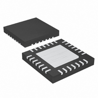
MAX8631XETI+T Maxim Integrated Products, MAX8631XETI+T Datasheet - Page 13

MAX8631XETI+T
Manufacturer Part Number
MAX8631XETI+T
Description
IC LED DRVR WHITE BCKLGT 28-TQFN
Manufacturer
Maxim Integrated Products
Type
Backlight, White LED (Serial Interface)r
Datasheet
1.MAX8631YETIT.pdf
(15 pages)
Specifications of MAX8631XETI+T
Constant Current
Yes
Topology
Linear (LDO), Switched Capacitor (Charge Pump)
Number Of Outputs
8
Internal Driver
Yes
Type - Primary
Backlight, Flash/Torch
Type - Secondary
White LED
Frequency
1MHz
Voltage - Supply
2.7 V ~ 5.5 V
Voltage - Output
5V
Mounting Type
Surface Mount
Package / Case
28-TQFN Exposed Pad
Operating Temperature
-40°C ~ 85°C
Current - Output / Channel
200mA
Internal Switch(s)
Yes
Efficiency
85%
Lead Free Status / RoHS Status
Lead free / RoHS Compliant
Figure 5. Schematic for When Fewer than 8 LEDs Is Acceptable
Typical operating waveforms shown in the Typical
Operating Characteristics show input ripple current in
1x, 1.5x, and 2x mode.
As shown in Table 2, the LDO output voltages, LDO1
and LDO2 are pin-programmable by the logic states of
P1 and P2. P1 and P2 are tri-level inputs: IN, open, and
GND. The input voltage, V
selected LDO1 and LDO2 voltages. The logic states of
P1 and P2 can be programmed only during ENLDO
low. Once the LDO_ voltages are programmed, their
values do not change by changing P1 or P2 during
ENLDO high.
Use only ceramic capacitors with an X5R, X7R, or better
dielectric. See Table 3 for a list of recommended parts.
Connect a 1µF ceramic capacitor between LDO1 and
GND, and a second 1µF ceramic capacitor between
LDO2 and GND for 200mA applications. The LDO out-
put capacitor’s (C
(ESR) affects stability and output noise. Use output
capacitors with an ESR of 0.1Ω or less to ensure stability
and optimum transient response. Connect C
close to the MAX8631X/Y as possible to minimize the
impact of PC board trace inductance.
LDO Output Voltage Selection (P1 and P2)
1x/1.5x/2x White LED Charge Pump with Two
______________________________________________________________________________________
LDO
) equivalent series resistance
IN
Component Selection
INPUT
2.7V TO 5.5V
, must be greater than the
ON/OFF AND
SELECTION
VOLTAGE
10μF
6.81kΩ
LDOs in 4mm x 4mm Thin QFN
PIN
IN
GND
ENM2
ENM1
ENF
ENLDO
P1
P2
SETM
C1P
4.12kΩ
LDO_
1μF
C1N
SETF
MAX8631X
MAX8631Y
as
REFBP
C2P
0.01μF
1μF
C2N
The MAX8631X/Y is a high-frequency switched-capaci-
tor voltage regulator. For best circuit performance, use
a solid ground plane and place C
as close to the MAX8631X/Y as possible. There should
be no vias on C
exposed paddle directly under the IC. Refer to the
MAX8631X/Y evaluation kit for an example.
Table 2. P1 and P2, LDO Output Voltage
Selection
OPEN
OPEN OPEN
OPEN
PGND
LDO1
LDO2
GND
GND
GND
OUT
P1
IN
IN
IN
M1
M2
M3
M4
F1
F2
F3
F4
OPEN
OPEN
GND
GND
GND
1μF
10μF
P2
IN
IN
IN
UP TO 240mA
OUTPUT
1μF
MAIN
LDO1 (V)
IN
PC Board Layout and Routing
3.3
3.0
2.8
3.3
2.6
2.6
3.0
2.8
2.5
MAX8631X
. Connect GND and PGND to the
FLASH
LDO2 (V)
1.8
1.5
1.5
1.5
1.8
1.5
1.8
1.8
1.8
IN
, C
LDO1 (V)
OUT
2.8
2.8
2.9
2.6
2.6
2.8
2.9
2.9
2.9
MAX8631Y
, C3, and C4
LDO2 (V)
2.6
2.8
1.5
1.9
2.6
1.9
1.8
1.9
2.9
13


