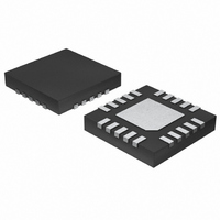
MAX16834ATP/V+ Maxim Integrated Products, MAX16834ATP/V+ Datasheet - Page 15

MAX16834ATP/V+
Manufacturer Part Number
MAX16834ATP/V+
Description
IC LED DRIVR HIGH BRIGHT 20-TQFN
Manufacturer
Maxim Integrated Products
Type
HBLED Driverr
Datasheet
1.MAX16834ATP.pdf
(23 pages)
Specifications of MAX16834ATP/V+
Topology
PWM, SEPIC, Step-Down (Buck), Step-Up (Boost)
Number Of Outputs
1
Internal Driver
No
Type - Primary
Automotive, Backlight
Type - Secondary
High Brightness LED (HBLED), RGB
Frequency
100kHz ~ 1MHz
Voltage - Supply
4.75 V ~ 28 V
Mounting Type
Surface Mount
Package / Case
20-TQFN Exposed Pad
Operating Temperature
-40°C ~ 125°C
Internal Switch(s)
Yes
Lead Free Status / RoHS Status
Lead free / RoHS Compliant
Voltage - Output
-
Current - Output / Channel
-
Efficiency
-
Lead Free Status / Rohs Status
Details
lowing equation. The MOSFET must be mounted on a
board as per manufacturer specifications to dissipate
the heat.
The RMS current rating of the switching MOSFET Q1 is
calculated as follows for boost and boost-buck configu-
rations:
where ID
amperes.
The MOSFET Q1 will dissipate power due to both
switching losses as well as conduction losses. The con-
duction losses in the MOSFET is calculated as follows:
where R
an assumed junction temperature of +100°C, P
in watts, and IL
Use the following equations to calculate the switching
losses in the MOSFET:
Boost configuration:
Boost-buck configuration:
where IG
MOSFET Q1 in amperes when it is turned on and
turned off, respectively, V
IL
gate-to-drain MOSFET capacitance in farads.
Choose a MOSFET that has a higher power rating than
that calculated by the following equation when the
MOSFET case temperature is at +70°C:
High-Power LED Driver with Integrated High-Side LED
AVG
Current Sense and PWM Dimming MOSFET Driver
P
SW
is in amperes, f
=
DSON
×
ID
RMS
P
ON
P
⎛
⎜
⎝
SW
⎛
⎝ ⎜
RMS
COND
IL
P
I
G G
TOT
AVG
is the MOSFET Q1’s drain RMS current in
and IG
=
1
ON
×
is the on-resistance of Q1 in ohms with
AVG
⎛
⎜
⎝
=
⎛
⎝ ⎜
( )
IL
=
W
⎛
⎝ ⎜
IG
×
______________________________________________________________________________________
+
(
AVG
is in amperes.
(
IG
IL
1
ON
V
(
OFF
=
IL
LED
AVG
OFF
1
P
AVG
SW
×
+
COND
V
IG
are the gate currents of the
+
LED
⎞
⎠ ⎟
)
LED
is in hertz, and C
2
)
V
OF
1
2
INMAX
×
( )
2
×
2
and V
W
F F
D
2
D
⎞
⎠ ⎟
MAX
×
+
MAX
C
P
)
GD
2
SW
INMAX
×
×
⎞
⎠ ⎟
R
×
( )
C
×
W
DSON
1 3 .
f
GD
SW
are in volts,
×
⎞
⎟
⎠
GD
f
SW
COND
is the
⎞
⎟
⎠
is
Use a Schottky diode as the rectifier (D1) for fast
switching and to reduce power dissipation. The select-
ed Schottky diode must have a voltage rating 20%
above the maximum converter output voltage. The max-
imum converter output voltage is V
ration and V
The current rating of the diode should be greater than
I
Select a dimming MOSFET (Q2) with continuous current
rating at +70°C, higher than the LED current by 30%.
The drain-to-source voltage rating of the dimming
MOSFET must be higher than V
The LED current control loop comprising of the switch-
ing converter, the LED current amplifier, and the error
amplifier should be compensated for stable control of
the LED current. The switching converter small-signal
transfer function has a right half-plane (RHP) zero for
both boost and boost-buck configurations as the induc-
tor current is in continuous conduction mode. The RHP
zero adds a 20dB/decade gain together with a 90°
phase lag, which is difficult to compensate. The easiest
way to avoid this zero is to roll off the loop gain to 0dB
at a frequency less than one-fifth of the RHP zero fre-
quency with a -20dB/decade slope.
The worst-case RHP zero frequency (f
ed as follows:
Boost configuration:
Boost-buck configuration:
where f
tance value of L1 in henries (H), and I
The switching converter small-signal transfer function
also has an output pole for both boost and boost-buck
configurations. The effective output impedance that
determines the output pole frequency together with the
output filter capacitance is calculated as:
D
in the following equation:
ZRHP
LED
f
is in hertz, V
ZRHP
f
I
ZRHP
D
+ V
=
IL
=
INMAX
=
AVG
2
V
V
π
Feedback Compensation
LED
LED
×
× ×
LED
2
in boost-buck configuration.
(
L I
1
π
-
×
×
× ×
D
(
is in volts, L is the induc-
L I
(
LED
1
MAX
1
LED
-
-
D
D
LED
LED
MAX
MAX
×
)
by 20%.
Dimming MOSFET
×
D
LED
1 5
MAX
ZRHP
in boost configu-
)
.
)
Rectifier Diode
2
2
is in amperes.
) is calculat-
15


