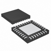
MAX16831ATJ+ Maxim Integrated Products, MAX16831ATJ+ Datasheet - Page 14

MAX16831ATJ+
Manufacturer Part Number
MAX16831ATJ+
Description
IC LED DRIVR HIGH BRIGHT 32-TQFN
Manufacturer
Maxim Integrated Products
Type
HBLED Driverr
Datasheet
1.MAX16831ATJT.pdf
(19 pages)
Specifications of MAX16831ATJ+
Topology
PWM, Step-Down (Buck), Step-Up (Boost)
Number Of Outputs
1
Internal Driver
No
Type - Primary
Automotive
Type - Secondary
High Brightness LED (HBLED), RGB
Frequency
125kHz ~ 600kHz
Voltage - Supply
5.5 V ~ 76 V
Mounting Type
Surface Mount
Package / Case
32-TQFN Exposed Pad
Operating Temperature
-40°C ~ 125°C
Internal Switch(s)
Yes
Efficiency
90%
Low Level Output Current
76 mA
High Level Output Current
67 mA
Operating Supply Voltage
5.5 V to 76 V
Maximum Supply Current
4.5 mA
Maximum Power Dissipation
2758 mW
Maximum Operating Temperature
+ 125 C
Mounting Style
SMD/SMT
Minimum Operating Temperature
- 40 C
Lead Free Status / RoHS Status
Lead free / RoHS Compliant
Voltage - Output
-
Current - Output / Channel
-
Lead Free Status / Rohs Status
Details
The minimum required inductance is a function of oper-
ating frequency, input-to-output voltage differential, and
the peak-to-peak inductor current (ΔI
allows for a lower inductor value while a lower ΔI
requires a higher inductor value. A lower inductor value
minimizes size and cost, improves large-signal tran-
sient response but reduces efficiency due to higher
peak currents and higher peak-to-peak output ripple
voltage for the same output capacitance. On the other
hand, higher inductance increases efficiency by reduc-
ing the ripple current, ΔI
due to extra turns can exceed the benefit gained from
lower ripple current levels, especially when the induc-
tance is increased without also allowing for larger
inductor dimensions. A good compromise is to choose
ΔI
saturating current is also important to avoid runaway
current during the output overload and continuous
short circuit. Select the I
mum peak current limit.
Buck configuration: In a buck configuration, the aver-
age inductor current does not vary with the input. The
worst-case peak current occurs at a high input voltage.
In this case, the inductance L for continuous conduc-
tion mode is given by:
where V
switching frequency, and V
Boost configuration: In the boost converter, the average
inductor current varies with line and the maximum aver-
age current occurs at low line. For the boost converter,
the average inductor current is equal to the input cur-
rent. In this case, the inductance L is calculated as:
where V
output voltage, and f
Buck-boost configuration: In a buck-boost converter,
the average inductor current is equal to the sum of the
input current and the load current. In this case, the
inductance L is:
High-Voltage, High-Power LED Driver with
Analog and PWM Dimming Control
14
L
equal to 30% of the full load current. The inductor
______________________________________________________________________________________
INMAX
INMIN
L
=
L
(
V
L
is the minimum input voltage, V
=
is the maximum input voltage, f
OUT
Applications Information
=
V
V
OUT
INMIN
V
V
+
SW
INMAX
OUT
V
V
×
INMIN
OUT
is the switching frequency.
SAT
(
V
×
L
×
INMAX
OUT
. However, resistive losses
(
×
V
V
×
to be higher than the maxi-
)
INMIN
f
OUT
f
×
SW
SW
Inductor Selection
is the output voltage.
f
SW
×
-
×
-
V
Δ
V
×
Δ
OUT
I
INMIN
I
L
Δ
L
I
L
L
)
). Higher ΔI
)
OUT
SW
is the
is the
L
L
where V
output voltage, and f
The function of the output capacitor is to reduce the
output ripple to acceptable levels. The ESR, ESL, and
the bulk capacitance of the output capacitor contribute
to the output ripple. In most of the applications, the out-
put ESR and ESL effects can be dramatically reduced
by using low-ESR ceramic capacitors. To reduce the
ESL effects, connect multiple ceramic capacitors in
parallel to achieve the required bulk capacitance.
In a buck configuration, the output capacitance, C
calculated using the following equation:
where ΔV
In a boost configuration, the output capacitance, C
calculated as:
where I
In a buck-boost configuration, the output capacitance,
C
where V
the output current. Connect the output capacitor(s)
from the output to ground in a buck-boost configuration
(not across the load as for other configurations).
A capacitor connected between the input line and
ground must be used when configuring the MAX16831
as a buck converter. Use a low-ESR input capacitor
that can handle the maximum input RMS ripple current.
Calculate the maximum allowable RMS ripple using the
following equation:
In most of the cases, an additional electrolytic capaci-
tor should be added to prevent input oscillations due to
line impedances.
F
, is calculated as:
I
IN RMS
OUT
INMIN
(
OUT
R
C
C
is the maximum allowable output ripple.
C
F
is the output current.
)
F
is the voltage across the load and I
F
≥
=
is the minimum input voltage, V
≥
≥
Δ
I
(
OUT
V
Δ
V
R
V
OUT
(
V
R
SW
×
INMAX
Δ
×
× × ×
2
(
V
V
×
2
-
R
is the switching frequency.
OUT
V
V
V
×
OUT
INMIN
OUT
L V
V
-
OUT
+
V
V
INMIN
V
OUT
×
×
INMAX
INMIN
)
(
Output Capacitor
I
V
× ×
×
OUT
INMIN
)
2
Input Capacitor
f
SW
×
)
V
I
×
×
OUT
OUT
f
f
-
SW
SW
V
OUT
2
OUT
)
OUT
is the
F
F
, is
, is
is


