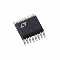
LT1768CGN Linear Technology, LT1768CGN Datasheet - Page 8

LT1768CGN
Manufacturer Part Number
LT1768CGN
Description
IC CTRLR CCFL SGL/MULT HP 16SSOP
Manufacturer
Linear Technology
Type
CCFL Controllerr
Datasheet
1.LT1768CGN.pdf
(20 pages)
Specifications of LT1768CGN
Frequency
300 ~ 410 kHz
Current - Supply
7mA
Current - Output
1.5A
Voltage - Supply
9 V ~ 24 V
Operating Temperature
0°C ~ 125°C
Package / Case
16-SSOP
Lead Free Status / RoHS Status
Contains lead / RoHS non-compliant
Available stocks
Company
Part Number
Manufacturer
Quantity
Price
Company:
Part Number:
LT1768CGN
Manufacturer:
LT
Quantity:
10 000
Part Number:
LT1768CGN
Manufacturer:
LINEAR/凌特
Quantity:
20 000
Part Number:
LT1768CGN#PBF
Manufacturer:
LINEAR/凌特
Quantity:
20 000
Part Number:
LT1768CGN#TRPBF
Manufacturer:
LINEAR/凌特
Quantity:
20 000
LT1768
R
of 1.25V that is to be loaded with an external resistor. The
current through the external resistor sets the maximum
lamp current. Maximum lamp current in a dual lamp
application will be approximately equal to 100 times I
when the voltage on the PROG pin is greater than 4V. The
value of R
[R
R
1.26V that is to be loaded with an external resistor. The
current through the external resistor sets the minimum
lamp current. Minimum lamp current in a dual lamp
application will be approximately 10 times the value of
I
and 1V. To set the minimum current to zero (I
for maximum dimming range, connect the R
V
connected to V
R
SHDN (Pin 12): The SHDN pin controls the operation of
the LT1768. Pulling the SHDN pin above 1.26V or leaving
the pin open will result in normal operation of the LT1768.
Pulling the SHDN pin below 1V causes a complete shut-
down of the LT1768 which results in a typical quiescent
current of 65 A. The SHDN pin has an internal 7 A pull-up
source to V
8
PIN
RMIN
REG
MAX
MIN
RMAX
RMIN
U
(Pin 11): The R
pin. The value of R
(Pin 10): The R
when the voltage on the PROG pin is between 0.5V
/[0.4 • (V
FUNCTIONS
• 2.5 • (V
RMAX
U
IN
and 200mV of voltage hysteresis.
REG
PWM–1
must be greater than 5K and less than
PWM–1
) must be greater than the value of
MIN
U
MAX
)/3] for proper PWM operation.
/3)] for proper PWM operation.
pin outputs a regulated voltage of
RMIN
pin outputs a regulated voltage
(R
RMIN
=
when R
MIN
RMIN
pin to the
= 0 A)
MIN
RMAX
is
FAULT (Pin 13): The FAULT pin is an open collector output
with a sink capability of 1mA that is activated when lamp
current falls below 125 A in either DIO1 or DIO2 for at least
1 full PWM cycle.
V
derived from the V
to 10mA of current to power external circuitry. During
undervoltage lockout, shutdown mode or thermal
shutdown, drive to the V
V
LT1768. For normal operation, the V
undervoltage lockout of 7.9V and below a maximum of 24V.
GATE (Pin 16): The GATE pin is the output of a NPN high
current output stage used to drive the gate of an external
MOSFET. It has a dynamic source and sink capability of
1.5A. During normal operation, the GATE pin is driven high
at the beginning of each oscillator period and then low
when the appropriate current in the switch is reached. The
GATE pin has a minimum on time of 125ns and a maximum
duty cycle of 93% at a frequency of 350kHz. For input
voltages less than 13V the gate will be driven to within 2V
of V
level will be clamped at a typical voltage of 12.5V.
REF
IN
IN
(Pin 15): The V
(Pin 14): The V
. For input voltages greater than 13V the gate pin high
IN
IN
REF
pin. The regulated voltage provides up
pin is the voltage supply pin for the
pin is a regulated 5V output that is
REF
pin will be disabled.
IN
pin must be above an


