IRS2166DPBF International Rectifier, IRS2166DPBF Datasheet - Page 2
IRS2166DPBF
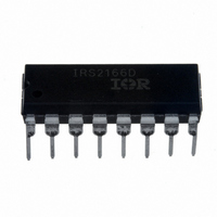
Manufacturer Part Number
IRS2166DPBF
Description
IC PFC/BALLAST/HALF BRDG 16-DIP
Manufacturer
International Rectifier
Type
PFC/Ballast Controllerr
Datasheet
1.IRS2166DSPBF.pdf
(18 pages)
Specifications of IRS2166DPBF
Frequency
40 ~ 46 kHz
Current - Supply
20mA
Current - Output
260mA
Voltage - Supply
12.5 V ~ 15.6 V
Operating Temperature
-25°C ~ 125°C
Package / Case
16-DIP (0.300", 7.62mm)
Package
16-pin DIP
Circuit
Fluorescent Ballast IC
Offset Voltage (v)
600
Output Source Current Min (ma)
180
Output Sink Current Min (ma)
260
Vcc Range (v)
10-20V with UVLO
Output Voltage Min (v)
10
Output Voltage Max (v)
20
Pbf
Yes
For Use With
IRPLLNR7 - KIT UNIV ELEC BALLAST FLUOR LAMP
Lead Free Status / RoHS Status
Lead free / RoHS Compliant
Available stocks
Company
Part Number
Manufacturer
Quantity
Price
Company:

Part Number:
IRS2166DPBF
Manufacturer:
IR
Quantity:
4 986
Part Number:
IRS2166DPBF
Manufacturer:
IR
Quantity:
20 000


www.irf.com
Recommended Operating Conditions
For proper operation the device should be used within the recommended conditions.
Absolute Maximum Ratings
Note 2: Enough current should be supplied into the V
regulating its voltage, V
Absolute maximum ratings indicate sustained limits beyond which damage to the device may occur. All voltage
parameters are absolute voltages referenced to COM, all currents are defined positive into any lead. The thermal
resistance and power dissipation ratings are measured under board mounted and still air conditions.
Symbol
voltage of 15.6 V. This supply pin should not be driven by a DC, low impedance power source greater than the V
specified in the electrical characteristics section.
Note 1: This IC contains a zener clamp structure between the chip V
V
I
I
dV/dt
I
V
V
SD/EOL
Symbol
V
V
R
O,MAX
V
I
COMP
SD/EOL
V
V
V
V
V
V
I
I
I
I
P
RPH
T
T
T
CPH
RPH
CC
PFC
BUS
RT
ZX
CS
ΘJA
HO
LO
RT
CT
CS
I
V
B
S
D
J
S
L
SD/EOL
V
I
B
V
C
I
I
T
CC
CS
ZX
-V
CC
S
T
J
S
High-side floating supply voltage
High-side floating supply offset voltage
High-side floating output voltage
Low-side output voltage
PFC gate driver output voltage
Maximum allowable output current (HO, LO, PFC) due to external
power transistor miller effect
VBUS pin voltage
CPH pin voltage
RT pin voltage
RPH pin voltage
RT pin current
RPH pin current
CT pin voltage
COMP pin current
ZX pin current
VCC pin current (see Note 1)
SD/EOL pin voltage
SD/EOL pin current
CS pin voltage
CS pin current
Allowable V
Package power dissipation @ T
PD = (T
Thermal resistance, junction to ambient
Junction temperature
Storage temperature
Lead temperature (soldering, 10 seconds)
High side floating supply voltage
Steady state high-side floating supply offset voltage
Supply voltage
V
CT pin capacitance
SD/EOL pin current
CS pin current
ZX pin current
Junction temperature
CC
JMAX
supply current (see Note 2)
CLAMP
-T
S
offset voltage slew rate
A
)/R
.
θJA
Definition
Definition
A
≤ +25 ºC
CC
pin to keep the internal 15.6 V zener clamp diode on this pin
(16-Pin DIP)
(16-Pin SOIC)
(16-Pin DIP)
(16-Pin SOIC)
CC
and COM which has a nominal breakdown
V
V
Note 2
Min.
V
V
Min.
S
B
-500
-0.3
-0.3
-0.3
-0.3
-0.3
-0.3
-0.3
-0.3
-0.3
-0.3
-25
-50
-55
-55
220
BSUV+
CCUV+
-25
---
---
---
---
---
-5
-5
-5
-5
-5
-5
- 0.3
-1
-1
– 25
IRS2166D(S)PbF
V
V
V
V
V
V
V
V
V
V
V
Max.
V
V
Max.
CC
CC
CC
CC
CC
CC
CC
CC
CC
B
B
600
125
625
500
150
150
300
CLAMP
CLAMP
1.8
1.4
20
25
50
70
82
---
+ 0.3
+ 0.3
5
5
5
5
5
1
+ 0.3
+ 0.3
+ 0.3
+ 0.3
+ 0.3
+ 0.3
+ 0.3
+ 0.3
5
+ 0.3
CLAMP
Units
Units
ºC/W
V/ns
mA
mA
mA
mA
mA
mA
mA
pF
ºC
ºC
W
V
V
V
V
V
V
Page 2
Related parts for IRS2166DPBF
Image
Part Number
Description
Manufacturer
Datasheet
Request
R

Part Number:
Description:
SCHOTTKY RECTIFIER
Manufacturer:
International Rectifier Corp.
Datasheet:
Part Number:
Description:
SCHOTTKY RECTIFIER
Manufacturer:
International Rectifier Corp.
Datasheet:
Part Number:
Description:
SCHOTTKY RECTIFIER
Manufacturer:
International Rectifier Corp.
Datasheet:
Part Number:
Description:
SCHOTTKY RECTIFIER
Manufacturer:
International Rectifier Corp.
Datasheet:
Part Number:
Description:
SCHOTTKY RECTIFIER
Manufacturer:
International Rectifier Corp.
Datasheet:
Part Number:
Description:
SCHOTTKY RECTIFIER
Manufacturer:
International Rectifier Corp.
Datasheet:
Part Number:
Description:
SCHOTTKY RECTIFIER
Manufacturer:
International Rectifier Corp.
Datasheet:
Part Number:
Description:
SCHOTTKY RECTIFIER
Manufacturer:
International Rectifier Corp.
Datasheet:
Part Number:
Description:
SCHOTTKY RECTIFIER
Manufacturer:
International Rectifier Corp.
Datasheet:
Part Number:
Description:
SCHOTTKY RECTIFIER
Manufacturer:
International Rectifier Corp.
Datasheet:
Part Number:
Description:
SCHOTTKY RECTIFIER
Manufacturer:
International Rectifier Corp.
Datasheet:
Part Number:
Description:
SCHOTTKY RECTIFIER
Manufacturer:
International Rectifier Corp.
Datasheet:
Part Number:
Description:
SCHOTTKY RECTIFIER
Manufacturer:
International Rectifier Corp.
Datasheet:
Part Number:
Description:
SCHOTTKY RECTIFIER
Manufacturer:
International Rectifier Corp.
Datasheet:
Part Number:
Description:
SCHOTTKY RECTIFIER
Manufacturer:
International Rectifier Corp.
Datasheet: