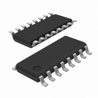
SI8234BB-C-IS1 Silicon Laboratories Inc, SI8234BB-C-IS1 Datasheet - Page 15

SI8234BB-C-IS1
Manufacturer Part Number
SI8234BB-C-IS1
Description
IC HIGH/LOW SIDE DRIVER 16SOIC
Manufacturer
Silicon Laboratories Inc
Specifications of SI8234BB-C-IS1
Configuration
High or Low Side
Input Type
Non-Inverting
Delay Time
60ns
Current - Peak
4A
Number Of Configurations
2
Number Of Outputs
2
Voltage - Supply
6.5 V ~ 24 V
Operating Temperature
-40°C ~ 125°C
Mounting Type
Surface Mount
Package / Case
16-SOIC (3.9mm Width)
Number Of Drivers
2
Driver Configuration
Non-Inverting
Driver Type
High and Low Side
Input Logic Level
TTL
Rise Time
12ns
Fall Time
12ns
Propagation Delay Time
30ns
Frequency (max)
8MHz
Operating Supply Voltage (max)
5.5/24V
Peak Output Current
4A
Power Dissipation
1.2W
Output Resistance
2.7Ohm
Operating Supply Voltage (min)
4.5/6.5V
Operating Temp Range
-40C to 125C
Operating Temperature Classification
Automotive
Mounting
Surface Mount
Pin Count
16
Package Type
SOIC N
Lead Free Status / RoHS Status
Lead free / RoHS Compliant
High Side Voltage - Max (bootstrap)
-
Lead Free Status / Rohs Status
Compliant
Other names
336-1901-5
Available stocks
Company
Part Number
Manufacturer
Quantity
Price
Part Number:
SI8234BB-C-IS1R
Manufacturer:
SILICON LABS/芯科
Quantity:
20 000
3. Functional Description
The operation of an Si823x channel is analogous to that of an opto coupler and gate driver, except an RF carrier is
modulated instead of light. This simple architecture provides a robust isolated data path and requires no special
considerations or initialization at start-up. A simplified block diagram for a single Si823x channel is shown in
Figure 8.
A channel consists of an RF Transmitter and RF Receiver separated by a semiconductor-based isolation barrier.
Referring to the Transmitter, input A modulates the carrier provided by an RF oscillator using on/off keying. The
Receiver contains a demodulator that decodes the input state according to its RF energy content and applies the
result to output B via the output driver. This RF on/off keying scheme is superior to pulse code schemes as it
provides best-in-class noise immunity, low power consumption, and better immunity to magnetic fields. See
Figure 9 for more details.
A
Transmitter
control
Dead
time
OSCILLATOR
MODULATOR
Figure 8. Simplified Channel Diagram
RF
Figure 9. Modulation Scheme
Semiconductor-
Based Isolation
Barrier
Rev. 1.1
DEMODULATOR
Receiver
Modulation Signal
Output Signal
Input Signal
Driver
Gnd
V
DD
Si823x
0.5 to 4 A
peak
B
15


