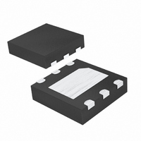
MAX5078BATT+T Maxim Integrated Products, MAX5078BATT+T Datasheet

MAX5078BATT+T
Specifications of MAX5078BATT+T
MAX5078BATT+TTR
Related parts for MAX5078BATT+T
MAX5078BATT+T Summary of contents
Page 1
... MAX5078A MAX5078B IN+ PWM IN IN- GND ________________________________________________________________ Maxim Integrated Products For pricing, delivery, and ordering information, please contact Maxim/Dallas Direct! at 1-888-629-4642, or visit Maxim’s website at www.maxim-ic.com. 4A, 20ns, MOSFET Driver ♦ 15V Single Power Supply ♦ 4A Peak Source/Sink Drive Current ♦ 20ns (typ) Propagation Delay ♦ ...
Page 2
MOSFET Driver ABSOLUTE MAXIMUM RATINGS (Voltages referenced to GND.) V ..............................................................................-0.3V to +18V DD IN+, IN- ........................................................................-0.3V to +18V OUT .................................................................-0. OUT Short-Circuit Duration.......................................................10ms Continuous Source/Sink Current at OUT_ (P Stresses beyond those listed under “Absolute ...
Page 3
ELECTRICAL CHARACTERISTICS (continued 15V -40°C to +125°C, unless otherwise noted. Typical values are PARAMETER Output-Voltage High LOGIC INPUT (Note 3) Logic 1 Input Voltage Logic 0 Input Voltage Logic-Input Hysteresis ...
Page 4
MOSFET Driver ELECTRICAL CHARACTERISTICS (continued 15V -40°C to +125°C, unless otherwise noted. Typical values are PARAMETER SYMBOL MATCHING CHARACTERISTICS Mismatch Propagation Delays from Inverting and Noninverting Inputs to ...
Page 5
A INPUT THRESHOLD VOLTAGE vs. SUPPLY VOLTAGE 10 MAX5078A 9 (CMOS INPUT RISING FALLING SUPPLY ...
Page 6
MOSFET Driver (T = +25°C, unless otherwise noted.) A LOGIC-INPUT VOLTAGE vs. OUTPUT VOLTAGE ( 40ns/div LOGIC-INPUT VOLTAGE vs. OUTPUT VOLTAGE ( 40ns/div 6 _______________________________________________________________________________________ Typical Operating Characteristics (continued) LOGIC-INPUT ...
Page 7
A LOGIC-INPUT VOLTAGE vs. OUTPUT VOLTAGE (V = 15V vs. OUTPUT VOLTAGE DD MAX5078B (TTL INPUT) _______________________________________________________________________________________ 4A, 20ns, MOSFET Driver Typical Operating Characteristics (continued) LOGIC-INPUT VOLTAGE vs. OUTPUT VOLTAGE = ...
Page 8
MOSFET Driver PIN NAME 1 IN- Inverting Logic-Input Terminal. Connect to GND when not used GND Ground 4 V Power Supply. Bypass to GND with one or more 0.1µF ceramic capacitors OUT Driver Output. ...
Page 9
IN OUT t D-OFF1 IN D-OFF2 RISING MISMATCH = D-ON2 D-ON1 FALLING MISMATCH = D-OFF2 D-OFF1 Figure 1. Timing Diagram Use the following equation to ...
Page 10
MOSFET Driver Table 1. MAX5078 Truth Table IN+ IN- Low Low Low High High Low High High Use the following PC board layout guidelines when designing with the MAX5078A/MAX5078B: • Place one or more 0.1µF decoupling ceramic capacitors ...
Page 11
TO 15V V DD IN+ MAX5078A MAX5078B OUT IN- FROM PWM GND CONTROLLER (BOOST IN+ MAX5078A MAX5078B OUT IN- GND Figure 6. MAX5078A/MAX5078B In High-Power Synchronous Buck Converter 15V V DD MAX5078 PWM ...
Page 12
... Maxim cannot assume responsibility for use of any circuitry other than circuitry entirely embodied in a Maxim product. No circuit patent licenses are implied. Maxim reserves the right to change the circuitry and specifications without notice at any time. 12 ____________________Maxim Integrated Products, 120 San Gabriel Drive, Sunnyvale, CA 94086 408-737-7600 © 2005 Maxim Integrated Products D ...


