NCP5181PG ON Semiconductor, NCP5181PG Datasheet
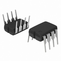
IC MOSFET DRVR HIGH VOLT 8-DIP

NCP5181PG

Manufacturer Part Number
NCP5181PG
Description
IC MOSFET DRVR HIGH VOLT 8-DIP
Manufacturer
ON Semiconductor
Type
High Side/Low Sider
Datasheet

Specifications of NCP5181PG

Configuration
Half Bridge
Input Type
Non-Inverting
Delay Time
100ns
Current - Peak
1.4A
Number Of Configurations
1
Number Of Outputs
2
High Side Voltage - Max (bootstrap)
600V
Voltage - Supply
10 V ~ 20 V
Operating Temperature
-40°C ~ 125°C
Mounting Type
Through Hole
Package / Case
8-DIP (0.300", 7.62mm)
Rise Time
60 ns
Fall Time
40 ns
Supply Voltage (min)
10 V
Supply Current
6.5 mA
Maximum Power Dissipation
100 mW
Maximum Operating Temperature
+ 150 C
Mounting Style
Through Hole
Bridge Type
Full Bridge, Half Bridge
Minimum Operating Temperature
- 55 C
Number Of Drivers
2
Lead Free Status / RoHS Status
Lead free / RoHS Compliant

Available stocks

Company
Part Number
Manufacturer
Quantity
Price
Part Number:
NCP5181PG
Manufacturer:
ON
Quantity:
4 660
Part Number:
NCP5181PG
Manufacturer:
ON/安森美
Quantity:
20 000
NCP5181
High Voltage High and Low
Side Driver
two outputs for direct drive of 2 N- -channel power MOSFETs arranged
in a half- -bridge (or any other high- -side + low- -side) configuration.
High- -side power switch. The driver works with 2 independent inputs
to accommodate any topology (including half- -bridge, asymmetrical
half- -bridge, active clamp and full- -bridge).
Features
Applications
 Semiconductor Components Industries, LLC, 2010
November, 2010 - - Rev. 6
PIN ASSIGNMENT
IN_HI
IN_LO
GND
DRV_LO
V
V
DRV_HI
BRIDGE
The NCP5181 is a High Voltage Power MOSFET Driver providing
It uses the bootstrap technique to insure a proper drive of the
active clamp)
High Voltage Range: up to 600 V
dV/dt Immunity 50 V/nsec
Gate Drive Supply Range from 10 V to 20 V
High and Low DRV Outputs
Output Source / Sink Current Capability 1.4 A / 2.2 A
3.3 V and 5 V Input Logic Compatible
Up to V
Matched Propagation Delays between Both Channels
Outputs in Phase with the Inputs
Independent Logic Inputs to Accommodate All Topologies
Under V
Pin to Pin Compatible with IR2181(S)
These are Pb- -Free Devices
High Power Energy Management
Half- -bridge Power Converters
Any Complementary Drive Converters (asymmetrical half- -bridge,
Full- -bridge Converters
Bridge Inverters for UPS Systems
CC
BOOT
PIN
CC
CC
Swing on Input Pins
LockOut (UVLO) for Both Channels
Logic Input for High Side Driver Output In Phase
Logic Input for Low Side Driver Output In Phase
Ground
Low Side Gate Drive Output
Low Side and Main Power Supply
Bootstrap Power Supply
High Side Gate Drive Output
Bootstrap Return or High Side Floating Supply Return
FUNCTION
1
†For information on tape and reel specifications,
NCP5181PG
NCP5181DR2G
including part orientation and tape sizes, please
refer to our Tape and Reel Packaging Specification
Brochure, BRD8011/D.
Device
CASE 751
D SUFFIX
8
1
DRV_LO
8
SOIC- -8
NCP5181P,
5181
A
L
Y, YY
W, WW = Work Week
G or G
IN_LO
ORDERING INFORMATION
IN_HI
ALYWX
GND
5181
MARKING DIAGRAMS
1
G
http://onsemi.com
= Specific Device Code
= Assembly Location
= Wafer Lot
= Year
= Pb--Free Package
(Pb--Free)
(Pb--Free)
Package
SOIC--8
PDIP--8
Publication Order Number:
2.500/Tape & Reel
CASE 626
P SUFFIX
NCP5181P
PDIP- -8
50 Units/Tube
V
DRV_HI
BRIDGE
V
BOOT
CC
Shipping
YYWWG
NCP5181/D
AWL

Related parts for NCP5181PG

NCP5181PG Summary of contents

Page 1

... Wafer Lot Year Work Week Pb--Free Package ORDERING INFORMATION Device Package NCP5181PG PDIP--8 (Pb--Free) NCP5181DR2G SOIC--8 (Pb--Free) †For information on tape and reel specifications, including part orientation and tape sizes, please refer to our Tape and Reel Packaging Specification Brochure, BRD8011/D. ...

Page 2

V bulk C1 GND GND 1 SG3526 IN_HI 2 MC34025 IN_LO TL594 3 GND NCP51XX GND GND DETECT IN_HI GND DELAY IN_LO GND GND GND ...

Page 3

MAXIMUM RATINGS Rating Main Power Supply Voltage VHV: High Voltage BOOT Pin VHV: High Voltage BRIDGE Pin VHV: Floating Supply Voltage VHV: High Side Output Voltage Low Side Output Voltage Allowable Output Slew Rate Inputs IN_HI, IN_LO ESD Capability: Human ...

Page 4

ELECTRICAL CHARACTERISTICS Rating OUTPUT SECTION Output High Short Circuit pulsed Current  10 ms, (Note 1) DRV Output Low Short Circuit Pulsed Current  10 ms, (Note 1) DRV CC ...

Page 5

IN_HI IN_LO DRV_HI DRV_LO Figure 3. Input/Output Timing Diagram 50% IN_HI IN_LO DRV_HI DRV_LO 10% Figure 4. Switching Time Waveform Definitions IN_LO 50% IN_HI t on Delta_t DRV_HI 10% t off 90% DRV_LO Figure 5. Delay ...

Page 6

High Side on 120 100 --40 -- TEMPERATURE (C) Figure 7. Turn- -on Propagation Delay vs. Temperature 180 160 t High Side off 140 120 100 t Low ...

Page 7

High Side Low Side 5.0 0 --40 -- TEMPERATURE (C) Figure 13. Turn- -on Rise Time vs. Temperature Low Side f 20 ...

Page 8

TEMPERATURE (C) Figure 18. Low Level Input Voltage Threshold vs. Temperature 2.5 2.0 1.5 1.0 0.5 0 --40 -- TEMPERATURE (C) Figure ...

Page 9

TEMPERATURE (C) Figure 24. High Side Supply Current vs. Temperature 500 400 300 200 100 0 --40 -- TEMPERATURE (C) Figure 26. V Supply ...

Page 10

load Ω gate 5 100 200 300 400 SWITCHING FREQUENCY (kHz) Figure 30. ICC1 Consumption vs. Switching Frequency with 15 ...

Page 11

... S B 0.25 (0.010 - SEATING PLANE - - 0.25 (0.010 *For additional information on our Pb--Free strategy and soldering details, please download the ON Semiconductor Soldering and Mounting Techniques Reference Manual, SOLDERRM/D. PACKAGE DIMENSIONS SOIC CASE 751--07 ISSUE 0.10 (0.004 SOLDERING FOOTPRINT* 1.52 0.060 7.0 4.0 0.275 ...

Page 12

... Equal Opportunity/Affirmative Action Employer. This literature is subject to all applicable copyright laws and is not for resale in any manner. PUBLICATION ORDERING INFORMATION LITERATURE FULFILLMENT: Literature Distribution Center for ON Semiconductor P.O. Box 5163, Denver, Colorado 80217 USA Phone: 303--675--2175 or 800--344--3860 Toll Free USA/Canada Fax: 303--675--2176 or 800--344--3867 Toll Free USA/Canada Email: orderlit@onsemi ...

Related keywords