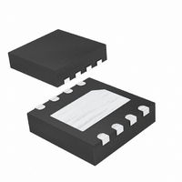
MAX5054BATA+T Maxim Integrated Products, MAX5054BATA+T Datasheet - Page 12

MAX5054BATA+T
Manufacturer Part Number
MAX5054BATA+T
Description
IC MOSFET DRVR DUAL 8-TDFN
Manufacturer
Maxim Integrated Products
Type
Low Sider
Datasheet
1.MAX5054AATAT.pdf
(15 pages)
Specifications of MAX5054BATA+T
Configuration
Low-Side
Input Type
Differential
Delay Time
20ns
Current - Peak
4A
Number Of Configurations
2
Number Of Outputs
2
Voltage - Supply
4 V ~ 15 V
Operating Temperature
-40°C ~ 125°C
Mounting Type
Surface Mount
Package / Case
8-TDFN Exposed Pad
Rise Time
85 ns
Fall Time
75 ns
Supply Voltage (min)
4 V
Supply Current
2.4 mA
Maximum Power Dissipation
1454 mW
Maximum Operating Temperature
+ 125 C
Mounting Style
SMD/SMT
Maximum Turn-off Delay Time
35 ns
Maximum Turn-on Delay Time
35 ns
Minimum Operating Temperature
- 40 C
Number Of Drivers
2
Lead Free Status / RoHS Status
Lead free / RoHS Compliant
High Side Voltage - Max (bootstrap)
-
Lead Free Status / Rohs Status
Lead free / RoHS Compliant
Other names
MAX5054BATA+T
MAX5054BATA+TTR
MAX5054BATA+TTR
Both the SO-EP and TDFN-EP packages have an
exposed pad on the bottom of their package. These
pads are internally connected to GND. For the best
thermal conductivity, solder the exposed pad to the
4A, 20ns, Dual MOSFET Drivers
Figure 5. Push-Pull Converter with Synchronous Rectification Drive Using MAX5054
12
PWM IN
PWM IN
______________________________________________________________________________________
INA+
INA-
INB+
INB-
MAX5054
V
IN
OUTA
OUTB
GND
V
DD
V
DD
Exposed Pad
PWM IN
ground plane to dissipate 1.5W and 1.9W in SO-EP and
TDFN-EP packages, respectively. Do not use the
ground-connected pads as the only electrical ground
connection or ground return. Use GND (pin 3) as the
primary electrical ground connection.
Additional Application Circuits
INA+
INA-
INB+
INB-
MAX5054
OUTA
OUTB
GND
V
DD
V
OUT


