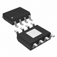
MAX15019BASA+ Maxim Integrated Products, MAX15019BASA+ Datasheet - Page 8

MAX15019BASA+
Manufacturer Part Number
MAX15019BASA+
Description
IC MOSF DRVR HALF BRDG HS 8-SOIC
Manufacturer
Maxim Integrated Products
Type
High Side/Low Sider
Datasheet
1.MAX15019BASA.pdf
(14 pages)
Specifications of MAX15019BASA+
Configuration
Half Bridge
Input Type
Inverting and Non-Inverting
Delay Time
36ns
Current - Peak
3A
Number Of Configurations
1
Number Of Outputs
2
High Side Voltage - Max (bootstrap)
125V
Voltage - Supply
8 V ~ 12.6 V
Operating Temperature
-40°C ~ 125°C
Mounting Type
Surface Mount
Package / Case
8-SOIC (3.9mm Width) Exposed Pad, 8-eSOIC. 8-HSOIC
Rise Time
50 ns
Fall Time
40 ns
Supply Voltage (min)
8 V
Supply Current
2.75 mA
Maximum Power Dissipation
1904 mW
Maximum Operating Temperature
+ 125 C
Mounting Style
SMD/SMT
Bridge Type
Half Bridge
Maximum Turn-off Delay Time
36 ns
Maximum Turn-on Delay Time
36 ns
Minimum Operating Temperature
- 40 C
Number Of Drivers
2
Lead Free Status / RoHS Status
Lead free / RoHS Compliant
125V/3A, High-Speed,
Half-Bridge MOSFET Drivers
The MAX15018A/MAX15018B/MAX15019A/MAX15019B
half-bridge, n-channel MOSFET drivers control high-
and low-side MOSFETs in high-voltage, high peak-cur-
rent applications and offer a high 125V voltage range
that allows ample margin above the 100V transient
specification of telecom standards. These drivers oper-
ate with an IC supply voltage of 8V to 12.6V, and con-
sume only 2.75mA of supply current during typical
switching operations. The MAX15018_/MAX15019_ pro-
vide 3A (typ) sink/source peak current per output and
are capable of operating with large capacitive loads
and with switching frequencies near 1MHz.
These drivers are intended to be used to drive the
high-side MOSFET without requiring an isolation device
such as an optocoupler or a drive transformer. The
high-side driver is controlled by a TTL/CMOS logic sig-
nal referenced to ground and is powered by a boot-
strap circuit formed by an integrated diode and an
external capacitor. Undervoltage lockout (UVLO) pro-
tection is provided for both the high- and low-side dri-
ver supplies (BST and V
hysteresis of 0.5V (typ).
The drivers are independently controlled and feature
exceptionally fast switching times, very short propaga-
tion delays (35ns typ), and matched propagation delay-
times (2ns typ) between drivers, making them ideally
suited for high-frequency applications. Internal logic cir-
cuitry prevents shoot-through during output state
changes and minimizes package power dissipation.
These devices are available with CMOS (V
logic-level inputs. The MAX15018A/MAX15018B accept
CMOS input logic levels, while the MAX15019A/
MAX15019B accept TTL input logic levels. For both ver-
sions, the logic inputs are protected against voltage
spikes up to +15V, regardless of V
Logic Inputs (IN_H, IN_L) section.
The MAX15018_/MAX15019_ are available with both
high-side and low-side noninverting logic inputs or with
noninverting high-side and inverting low-side logic inputs.
See the Functional Diagrams and Selector Guide . The
MAX15018A and MAX15019A are pin-for-pin replace-
ments for the HIP2100IB and HIP2101IB, respectively.
8
_______________________________________________________________________________________
Detailed Description
DD
) and includes a UVLO
DD
. See the Driver
DD
/2) or TTL
The MAX15018_/MAX15019_ are available in a space-
saving, high-power, 8-pin SO-EP package that can dissi-
pate up to 1.95W at +70°C. All devices operate over the
-40°C to +125°C automotive temperature range.
Both the high- and low-side drivers feature separate
UVLO protection that monitors each driver’s input sup-
ply voltage (BST and V
threshold (V
both driver outputs low when V
The high-side driver UVLO threshold (V
erenced to HS, and only pulls DH low when V
below 6.9V (typ) with respect to HS. After the IC is first
energized, and once V
old, DL starts switching and either follows the IN_L logic
input (MAX15018A/MAX15019A) or is inverted with refer-
ence to the IN_L logic input (MAX15018B/
MAX15019B). At this time, the bootstrap capacitor is not
charged, and DH does not switch since the BST-to-HS
voltage is below V
ing engagement of low-side switching, C
through V
DH then starts switching and follows IN_H. For synchro-
nous buck and half-bridge converter topologies, the
bootstrap capacitor can charge up in one cycle. Normal
operation then begins in a few microseconds after the
BST-to-HS voltage exceeds V
switch forward topology, C
hundred microseconds) to charge and increase its volt-
age above V
UVLO thresholds is 0.5V. The bootstrap capacitor value
should be selected carefully to avoid oscillations during
turn-on and turn-off at the DH output. Choose a capaci-
tor value 20 times greater than the total gate capaci-
tance of the MOSFET. Use a low ESR-type X7R
dielectric ceramic capacitor at BST (typically a 0.1µF
ceramic is adequate) and a parallel combination of 1µF
and 0.1µF ceramic capacitors from V
high-side MOSFET’s continuous on-time is limited due
to the charge loss from the high-side driver’s quiescent
current. The maximum on-time is dependent on the size
of C
BST
, I
BST
DD
DD_UVLO
BST_UVLO
(190µA, max), and V
and causes V
BST_UVLO
) is referenced to GND and pulls
DD
. The typical hysteresis for both
DD
rises above its UVLO thresh-
Undervoltage Lockout
). The low-side driver UVLO
BST
BST
. Within a short time follow-
DD
takes more time (a few
BST_UVLO
to exceed V
BST_UVLO
falls below 7.3V (typ).
DD
BST_UVLO
. In the two-
to GND. The
BST
.
BST_UVLO
BST
charges
) is ref-
falls
.


