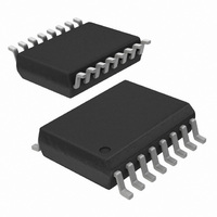
SI8232BD-B-IS Silicon Laboratories Inc, SI8232BD-B-IS Datasheet - Page 7

SI8232BD-B-IS
Manufacturer Part Number
SI8232BD-B-IS
Description
IC DUAL LOW SIDE DRIVER 16SOIC
Manufacturer
Silicon Laboratories Inc
Datasheet
1.SI8234BB-C-IS1.pdf
(52 pages)
Specifications of SI8232BD-B-IS
Package / Case
16-SOIC (0.300", 7.5mm Width)
Configuration
Low-Side
Input Type
Non-Inverting
Delay Time
60ns
Current - Peak
500mA
Number Of Configurations
2
Number Of Outputs
2
Voltage - Supply
6.5 V ~ 24 V
Operating Temperature
-40°C ~ 125°C
Mounting Type
Surface Mount
Mounting Style
SMD/SMT
Number Of Channels
2
Propagation Delay Time
30 ns
Supply Voltage (max)
5.5 V
Supply Voltage (min)
4.5 V
Supply Current
2 mA
Power Dissipation
1.2 W
Maximum Operating Temperature
+ 125 C
Minimum Operating Temperature
- 40 C
Lead Free Status / RoHS Status
Lead free / RoHS Compliant
High Side Voltage - Max (bootstrap)
-
Lead Free Status / Rohs Status
Lead free / RoHS Compliant
Other names
336-1908-5
Available stocks
Company
Part Number
Manufacturer
Quantity
Price
Company:
Part Number:
SI8232BD-B-ISR
Manufacturer:
KEMET
Quantity:
460 000
Table 1. Electrical Characteristics
4.5 V < VDDI < 5.5 V, VDDA = VDDB = 12 V or 15 V. TA = –40 to +125 °C. Typical specs at 25 °C
Parameter
VDDI Undervoltage Threshold
VDDI Undervoltage Threshold
VDDI Lockout Hysteresis
VDDA, VDDB Undervoltage
Threshold
5 V Threshold
8 V Threshold
10 V Threshold
12.5 V Threshold
VDDA, VDDB Undervoltage
Threshold
5 V Threshold
8 V Threshold
10 V Threshold
12.5 V Threshold
VDDA, VDDB
Lockout Hysteresis
VDDA, VDDB
Lockout Hysteresis
VDDA, VDDB
Lockout Hysteresis
AC Specifications
Minimum Pulse Width
Propagation Delay
Pulse Width Distortion
|t
Minimum Overlap Time
Programmed Dead Time
Output Rise and Fall Time
Notes:
PLH
1. VDDA = VDDB = 12 V for 5, 8, and 10 V UVLO devices; VDDA = VDDB = 15 V for 12.5 V UVLO devices.
2. TDD is the minimum overlap time without triggering overlap protection (Si8230/1/3/4 only).
3. The largest RDT resistor that can be used is 220 k.
- t
PHL
|
2
3
VDDA
VDDA
VDDA
VDDA
VDDA
VDDB
VDDB
VDDB
VDDB
VDDB
t
VDDI
VDDI
VDDI
Symbol
PHL
PWD
TDD
t
DT
R
, t
,t
1
HYS
UV+
UV–
HYS
HYS
HYS
UV+
UV–
F
HYS
HYS
HYS
PLH
UV+
UV–
(Continued)
,
,
,
,
,
UVLO voltage = 10 V or 12.5 V
C
See Figure 36 on page 25.
See Figure 37 on page 25.
See Figure 38 on page 25.
See Figure 39 on page 25.
See Figure 36 on page 25.
See Figure 37 on page 25.
See Figure 38 on page 25.
See Figure 39 on page 25.
C
DT = VDDI, No-Connect
L
Figure 41, RDT = 100 k
L
Figure 41, RDT = 6 k
= 200 pF (Si8233/4/5/6)
VDDA, VDDB falling
UVLO voltage = 5 V
UVLO voltage = 8 V
VDDA, VDDB rising
Rev. 1.1
= 200 pF (Si8230/1/2)
Test Conditions
CL = 200 pF
VDDI falling
VDDI rising
3.60
3.30
5.20
7.50
9.60
12.4
4.90
7.20
9.40
11.6
Min
—
—
—
—
—
—
—
—
—
—
—
—
1000
3.70
5.80
8.60
13.8
5.52
8.10
10.1
12.8
11.1
Typ
250
280
600
900
0.4
4.0
10
30
—
70
—
—
Si823x
5.60
Max
4.45
4.15
6.30
9.40
12.2
14.8
8.70
10.9
13.8
6.0
60
20
12
—
—
—
—
—
—
—
—
Units
mV
mV
mV
mV
ns
ns
ns
ns
ns
ns
ns
ns
V
V
V
V
V
V
V
V
V
V
7


