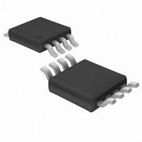
LTC1693-3CMS8#TRPBF Linear Technology, LTC1693-3CMS8#TRPBF Datasheet - Page 9

LTC1693-3CMS8#TRPBF
Manufacturer Part Number
LTC1693-3CMS8#TRPBF
Description
IC MOSFET DVR N-CH SINGLE 8-MSOP
Manufacturer
Linear Technology
Datasheet
1.LTC1693-1CS8PBF.pdf
(20 pages)
Specifications of LTC1693-3CMS8#TRPBF
Configuration
High-Side
Input Type
Inverting and Non-Inverting
Delay Time
38ns
Current - Peak
1.5A
Number Of Configurations
1
Number Of Outputs
1
Voltage - Supply
4.5 V ~ 13.2 V
Operating Temperature
0°C ~ 70°C
Mounting Type
Surface Mount
Package / Case
8-MSOP, Micro8™, 8-uMAX, 8-uSOP,
Lead Free Status / RoHS Status
Lead free / RoHS Compliant
High Side Voltage - Max (bootstrap)
-
Available stocks
Company
Part Number
Manufacturer
Quantity
Price
APPLICATIONS
Driver Electrical Isolation
The LTC1693-1 and LTC1693-2 incorporate two individual
drivers in a single package that can be separately connected
to GND and V
an LTC1693-2, its top driver left floating while the bottom
Figure 2. Simplified LTC1693-2 Floating Driver Application
GND1
GND2
GND1
GND2
IN1
IN2
IN1
IN2
Figure 3. Simplified LTC1693-1 Application
with Different Ground Potentials
CC
LTC1693-2
LTC1693-1
connections. Figure 2 shows a circuit with
U
PRIMARY-SIDE
CIRCUITS
OTHER
INFORMATION
V
OUT1
V
OUT2
U
V
OUT1
V
OUT2
CC1
CC2
CC1
CC2
V
V
+
+
•
W
1693 F03
•
SECONDARY-SIDE
CIRCUITS
OTHER
•
V
U
IN
N1
N2
1693 F02
V
+
driver is powered with respect to ground. Similarly Figure
3 shows a simplified circuit of a LTC1693-1 which is driv-
ing MOSFETs with different ground potentials. Because
there is 1G of isolation between these drivers in a single
package, ground current on the secondary side will not
recirculate to the primary side of the circuit.
Power Dissipation
To ensure proper operation and long term reliability, the
LTC1693 must not operate beyond its maximum tempera-
ture rating. Package junction temperature can be calcu-
lated by:
where:
Power dissipation consists of standby and switching
power losses:
where:
The LTC1693 consumes very little current during standby.
This DC power loss per driver at V
(360 A)(12V) = 4.32mW.
AC switching losses are made up of the output capacitive
load losses and the transition state losses. The capactive
load losses are primarily due to the large AC currents
needed to charge and discharge the load capacitance
during switching. Load losses for the CMOS driver driving
a pure capacitive load C
The power MOSFET’s gate capacitance seen by the driver
output varies with its V
A power MOSFET’s capacitive load power dissipation can
be calculated by its gate charge factor, Q
T
T
T
PD = Power Dissipation
PD = PSTDBY + PAC
PSTDBY = Standby Power Losses
PAC = AC Switching Losses
Load Capacitive Power (C
J
J
A
JA
= T
= Junction Temperature
= Ambient Temperature
= Junction-to-Ambient Thermal Resistance
A
+ PD(
JA
)
GS
OUT
voltage level during switching.
will be:
OUT
) = (C
OUT
CC
LTC1693
G
)(f)(V
= 12V is only
. The Q
CC
)
G
2
value
9


