IR2304SPBF International Rectifier, IR2304SPBF Datasheet
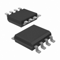
IC DRIVER HALF BRIDGE 8-SOIC

IR2304SPBF

Manufacturer Part Number
IR2304SPBF
Description
IC DRIVER HALF BRIDGE 8-SOIC
Manufacturer
International Rectifier
Datasheet

Specifications of IR2304SPBF

Configuration
High and Low Side, Independent
Input Type
Non-Inverting
Delay Time
220ns
Current - Peak
60mA
Number Of Configurations
1
Number Of Outputs
2
High Side Voltage - Max (bootstrap)
600V
Voltage - Supply
10 V ~ 20 V
Operating Temperature
-40°C ~ 125°C
Mounting Type
Surface Mount
Package / Case
8-SOIC (3.9mm Width)
Number Of Drivers
2
Driver Configuration
Non-Inverting
Driver Type
High and Low Side
Input Logic Level
CMOS/LSTTL
Rise Time
300ns
Fall Time
170ns
Propagation Delay Time
330ns
Operating Supply Voltage (max)
20V
Peak Output Current
130uA
Power Dissipation
625mW
Operating Supply Voltage (min)
10V
Turn Off Delay Time
50fs
Turn On Delay Time (max)
50ns
Operating Temp Range
-40C to 125C
Operating Temperature Classification
Automotive
Mounting
Surface Mount
Pin Count
8
Package Type
SOIC
Lead Free Status / RoHS Status
Lead free / RoHS Compliant
www.irf.com
Features
Description
The IR2304(S) are a high voltage, high speed
power MOSFET and IGBT driver with inde-
pendent high and low side referenced output
channels. Proprietary HVIC and latch immune
CMOS technologies
enable ruggedized monolithic construction.
The logic input is compatible with standard
CMOS or LSTTL output, down to 3.3V logic.
The output driver features a high pulse cur-
rent buffer stage designed for minimum driver
cross-conduction. The floating channel can be
used to drive an N-channel power MOSFET
or IGBT in the high side configuration which
operates up to 600 volts.
Block Diagram
Floating channel designed for bootstrap operation
to +600V. Tolerant to negative transient voltage
dV/dt immune
Gate drive supply range from 10 to 20V
Under voltage lockout for both channels
3.3V, 5V, and 15V input logic input compatible
Cross-conduction prevention logic
Matched propagation delay for both channels
Lower di/dt gate driver for better noise immunity
Internal 100ns dead-time
Output in phase with input
Available in Lead-Free
HIN
Vcc
LIN
COM
HIN
VCC
LIN
IR2304
HO
VB
VS
LO
2106/2301/2108/2109/2302/2304 Feature Comparison
2106/2301
2109/2302
21064
21084
21094
2108
2304
Part
Package
Product Summary
Internal deadtime
HIN/LIN
HIN/LIN
HIN/LIN
Delay Matching
IN/SD
Input
logic
t
I
on/off
V
O +/-
HALF-BRIDGE DRIVER
OFFSET
V
OUT
8-Lead PDIP
conduction
prevention
(min)
IR2304(S) & (PbF)
(typ.)
Cross-
logic
yes
yes
yes
no
Data Sheet No. PD60200 revB
up to 600V
Programmable 0.54~5 µs
Internal 100ns
Internal 540ns
Internal 540ns
Dead-Time
60 mA/130 mA
none
220/220 ns
600V max.
10 - 20V
TO
LOAD
100 ns
50 ns
8 Lead SOIC
Ground Pins
VSS/COM
VSS/COM
VSS/COM
COM
COM
COM
COM
1

Related parts for IR2304SPBF

IR2304SPBF Summary of contents

Page 1

Features • Floating channel designed for bootstrap operation to +600V. Tolerant to negative transient voltage dV/dt immune • Gate drive supply range from 10 to 20V • Under voltage lockout for both channels • 3.3V, 5V, and 15V input logic ...

Page 2

IR2304(S)&(PbF) Absolute Maximum Ratings Absolute maximum ratings indicate sustained limits beyond which damage to the device may occur. All voltage param- eters are absolute voltages referenced to COM, all currents are defined positive into any lead. The thermal resistance and ...

Page 3

Static Electrical Characteristics 15V and T = 25°C unless otherwise specified. The V BIAS COM. The V and I parameters are referenced to COM and Symbol Definition V ...

Page 4

IR2304(S)&(PbF) Functional Block Diagram 2304 HIN SHOOT- THROUGH PREVENTION LIN Lead Definitions Symbol Description V Low side supply voltage CC COM Logic ground and low side driver return HIN Logic input for high side gate driver output LIN Logic input ...

Page 5

Lead Assignments LIN 1 HIN 2 VCC 3 4 COM 8-Lead PDIP HIN LIN HO Internal Deadtime LO Figure 1. Input/Output Functionality Diagram www.irf.com IR2304(S)&(PbF) LIN VB 8 ...

Page 6

IR2304(S)&(PbF) 50% HIN LIN HIN 50% LIN 10 90% 6 50% t off t r 90% 90% 10% Figure 2. Switching Time Waveforms 50% 90% DT 10% Figure 3. Internal Deadtime Timing t ...

Page 7

Case outlines 0.25 [.010 0.25 [.010 NOT ES: 1. DIMENS IONING & TOLE RANCING PE R ...

Page 8

... This product has been designed and qualified for the Industrial market. Qualification Standards can be found on IR’s Web Site. Data and specifications subject to change without notice. Visit us at www.irf.com for sales contact information. order IR2304PbF order IR2304SPbF TAC Fax: (310) 252-7903 09/10/04 www.irf.com ...

Related keywords