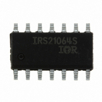
IRS21064SPBF International Rectifier, IRS21064SPBF Datasheet

IRS21064SPBF
Specifications of IRS21064SPBF
Available stocks
Related parts for IRS21064SPBF
IRS21064SPBF Summary of contents
Page 1
Features Floating channel designed for bootstrap operation Fully operational to +600 V Tolerant to negative transient voltage, dV/dt immune Gate drive supply range from Undervoltage lockout for both channels 3 and 15 ...
Page 2
Absolute Maximum Ratings Absolute maximum ratings indicate sustained limits beyond which damage to the device may occur. All voltage param- eters are absolute voltages referenced to COM. The thermal resistance and power dissipation ratings are measured under board mounted and ...
Page 3
Recommended Operating Conditions The input/output logic timing diagram is shown in Fig. 1. For proper operation the device should be used within the recommended conditions. The V and V S Symbol VB High-side floating supply absolute voltage V High-side floating ...
Page 4
Static Electrical Characteristics COM and T BIAS referenced to V /COM and are applicable to the respective input leads. The COM and are applicable ...
Page 5
Functional Block Diagrams IRS2106 HIN LIN IRS21064 HIN LIN VSS www.irf.com IRS2106/IRS21064(S)PbF PULSE HV FILTER LEVEL SHIFTER VSS/COM LEVEL PULSE SHIFT GENERATOR VSS/COM LEVEL DELAY SHIFT PULSE HV FILTER LEVEL SHIFTER VSS/COM LEVEL PULSE SHIFT GENERATOR VSS/COM LEVEL DELAY SHIFT ...
Page 6
... CC LO Low-side gate drive output COM Low-side return Lead Assignments HIN LIN LO 4 COM 8 Lead PDIP IRS2106PbF HIN 3 LIN 4 5 VSS 6 COM Lead PDIP IRS21064PbF www.irf.com IRS2106/IRS21064(S)PbF HIN LIN COM 8 Lead SOIC IRS2106SPbF HIN LIN VSS 9 6 COM Lead SOIC IRS21064SPbF 6 ...
Page 7
HIN LIN HO LO Figure 1. Input/Output Timing Diagram HIN LIN HO LO Figure 2. Switching Time Waveform Definitions www.irf.com IRS2106/IRS21064(S)PbF 50% 50 off 90% 90% 10% 10% 50% HIN LIN LO MT ...
Page 8
M ax 200 Typ. 100 0 -50 - Temperature ( Figure 4A. Turn-On Propagation Delay vs. Temperature 500 400 300 M ax. 200 Typ. 100 0 -50 - Temperature ( Figure ...
Page 9
Max. 100 Typ. 0 -50 - Temperature ( Figure 6A. Turn-On Rise Time vs. Temperature 200 150 100 Max. 50 Typ. 0 -50 - Temperature ( Figure 7A. Turn-Off Fall ...
Page 10
Max -50 - Temperature ( Figure 8A. Logic “1” Input Voltage vs. Temperature 4.0 3.2 2.4 1.6 M in. 0.8 0.0 -50 - ...
Page 11
Max. 0.1 Typ. 0.0 -50 - Temperature ( Figure 10A. High Level Output Voltage vs. Temperature 0.5 0.4 0.3 0.2 0.1 Max. Typ. 0.0 -50 - Temperature ( Figure 11A. ...
Page 12
M ax Temperature ( Figure 12A. Offset Supply Leakage Current vs. Temperature 400 300 200 M ax. 100 Typ ...
Page 13
M ax. Typ. 100 Temperature ( Figure 14A. Quiescent V CC Supply Current vs. Temperature ax. 10 Typ ...
Page 14
Max -50 - Temperature (°C) Figure 16A. Logic "0" Input Bias Current vs. Temperature ax. Typ in -50 - ...
Page 15
M ax. 10 Typ Temperature ( Figure 19 Undervoltage Threshold (+) vs. Temperature 500 400 Typ. 300 200 Max. 100 0 -50 -25 ...
Page 16
Typ. 600 400 Max. 200 0 -50 - Figure 22A. Output Sink Current vs. Temperature Typ ...
Page 17
Frequency (kHz) Figure 25. IRS2106 vs. Frequency (IRFBC30 =15 V gate CC 140 120 100 Frequency (kHz) ...
Page 18
Frequency (kHz) Figure 29. IRS21064 vs. Frequency (IRFBC30 =15 V gate CC 140 120 100 Frequency (kHz) Figure 31. IRS21064 vs. ...
Page 19
Frequency (kHz) Figure 33. IRS2106S vs. Frequency (IRFBC30 =15 V gate CC 140 120 100 Frequency (kHz) Figure 35. IRS2106S vs. ...
Page 20
Frequency (kHz) Figure 37. IRS21064S vs. Freque ncy (IRFBC30 Figure 39. IRS21064S vs. Frequency (IRFPE50), www.irf.com ...
Page 21
Case Outlines 0.25 [.010 0.25 [.010 NOTES: 1. DIMENSIONING & TOLERANCING PER ASME Y14.5M-1994. 2. CONTROLLING ...
Page 22
IRS2106/IRS21064(S)PbF 14 Lead PDIP 14 Lead SOIC (narrow body) 01-6010 01-3002 03 (MS-001AC) 01-6019 01-3063 00 (MS-012AB) 22 ...
Page 23
Tape & Reel 8-lead SOIC NTROLLING D IM ENSION ...
Page 24
Tape & Reel 14-lead SOIC NTROLLING D IM ENSION ...
Page 25
... SPN code) Assembly site code Per SCOP 200-002 14-Lead PDIP IRS21064PbF 14-Lead SOIC IRS21064SPbF 14-Lead SOIC Tape & Reel IRS21064STRPbF This product has been designed and qualified for the industrial level. Qualification standards can be found at www.irf.com Data and specifications subject to change without notice. 12/4/2006 ...


