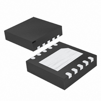
MAX15025AATB+T Maxim Integrated Products, MAX15025AATB+T Datasheet - Page 10

MAX15025AATB+T
Manufacturer Part Number
MAX15025AATB+T
Description
IC GATE DRVR 2CH 16NS 10TDFN-EP
Manufacturer
Maxim Integrated Products
Type
High Speedr
Datasheet
1.MAX15024AATBVT.pdf
(16 pages)
Specifications of MAX15025AATB+T
Configuration
High-Side
Input Type
Non-Inverting
Delay Time
16ns
Current - Peak
2A
Number Of Configurations
2
Number Of Outputs
2
Voltage - Supply
4.5 V ~ 28 V
Operating Temperature
-40°C ~ 125°C
Mounting Type
Surface Mount
Package / Case
10-TDFN Exposed Pad
Rise Time
48 ns
Fall Time
32 ns
Supply Current
1.5 mA
Maximum Power Dissipation
1481.5 mW
Maximum Operating Temperature
+ 125 C
Mounting Style
SMD/SMT
Maximum Turn-off Delay Time
18 ns
Maximum Turn-on Delay Time
18 ns
Minimum Operating Temperature
- 40 C
Number Of Drivers
2
Lead Free Status / RoHS Status
Lead free / RoHS Compliant
High Side Voltage - Max (bootstrap)
-
Lead Free Status / Rohs Status
Lead free / RoHS Compliant
Single/Dual, 16ns, High Sink/Source
Current Gate Drivers
10
The MAX15024 single gate driver’s internal source and
sink transistor outputs are brought out of the IC to inde-
pendent outputs allowing control of the external
MOSFET’s rise and fall time. The MAX15024 single
gate driver is capable of sinking an 8A peak current
and sourcing a 4A peak current. The MAX15025 dual
gate drivers are capable of sinking a 4A peak current
and sourcing a 2A peak current.
An integrated adjustable low-dropout linear voltage
regulator (LDO) provides gate drive amplitude control
and optimization. The single gate-driver propagation
delay time is minimized and matched between the
inverting and noninverting inputs. The dual gate-driver
propagation delay is matched between channels.
The MAX15024 has a dual input (IN+ and IN-), allows
the use of an inverting or noninverting input, and is
offered in TTL or CMOS-logic standards. The
MAX15025 is offered with configurations of inverting
and noninverting inputs with TTL or CMOS standards
(see the Selector Guide ).
The MAX15024/MAX15025 include an internal LDO
designed to deliver a stable reference voltage for use
as a supply voltage for the internal MOSFET gate dri-
vers. Connect the LDO feedback FB/SET to GND to set
V
divider between V
When V
channel transistor is ON and the internal p-channel tran-
sistor is OFF, holding the output at GND independent of
the state of the inputs so that the external MOSFETs
remain OFF in the UVLO condition. The UVLO threshold is
3.5V (typ) with 200mV (typ) hysteresis to avoid chattering.
When the device is operated at very low temperatures
and below the UVLO threshold, the driver output could
go high impedance. In this case, it is recommended
adding a 10kΩ resistor to PGND to discharge the gate
of the external MOSFET (see Figures 4 and 5).
REG
LDO Voltage Regulator Feedback Control
______________________________________________________________________________________
V
to a stable 10V. Connect FB/SET to a resistor-
REG
CC
= V
is below the UVLO threshold, the internal n-
FB/SET
REG
V
x (1 + R2 / R1) (see Figure 2)
Detailed Description
and GND to set V
CC
Undervoltage Lockout
REG
:
The MAX15024 features inverting and noninverting
input terminals. These inputs provide for flexibility of
design and use. Connect IN+ to V
an inverting input. Connect IN- to GND when using IN+
as a noninverting input.
The MAX15024/MAX15025 provide protection that
avoids any cross-conduction between the internal p-
channel and n-channel devices. It also eliminates shoot-
through, thus reducing the quiescent supply current.
The MAX15024/MAX15025 include an exposed pad
allowing greater heat dissipation from the internal die to
the outside environment. Solder the exposed pad care-
fully to GND or thermal pad to enhance the thermal
performance.
Ample supply bypassing and device grounding are
extremely important because when large external
capacitive loads are driven, the peak current at the
V
peak current can approach 8A. V
ground shifts are forms of negative feedback for invert-
ers and, if excessive, can cause multiple switching
when the inverting input is used and the input slew rate
is low. The device driving the input should be refer-
enced to the MAX15024/MAX15025 GND. Ground
shifts due to insufficient device grounding can disturb
other circuits sharing the same AC ground return path.
Any series inductance in the V
paths can cause oscillations due to the very high di/dt
that results when the MAX15024/MAX15025 are
switched with any capacitive load. A 0.1µF or larger
value ceramic capacitor is recommended for bypass-
ing V
pins as possible. When driving very large loads
(> 10nF) at minimum rise time, 10µF or more of parallel
storage capacitance is recommended. A ground plane
is highly recommended to minimize ground return resis-
tance and series inductance. Care should be taken to
place the MAX15024/MAX15025 as close as possible to
the external MOSFET being driven to further minimize
board inductance and AC path resistance.
DRV
DRV
pin can approach 4A, while at the PGND pin, the
Supply Bypassing, Device Grounding,
to GND and should be placed as close to the
Applications Information
Shoot-Through Protection
DRV
Exposed Pad (EP)
CC
, OUT_, and/or PGND
and Placement
when using IN- as
Input Control
DRV
drops and


